
Impedance afe

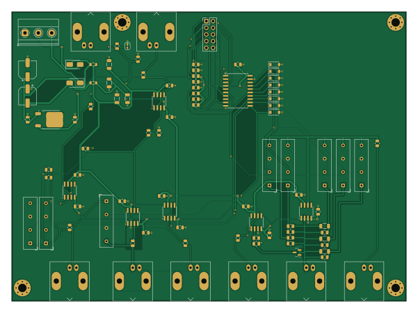
About the Impedance afe PCB
Impedance afe is an open source PCB design by byzantic, published on GitHub. It is a 2-layer board measuring 150 × 110 mm, with 93 components from 41 distinct parts.
Other key parts include the OPA828IDR, SN74HCT541DWR and MC78M05CDTRKG. By type, the board carries 27 capacitors, 27 resistors, 11 diodes, 10 connectors, 8 ICs and 8 relays.
It belongs with the test & measurement designs in this gallery.
From the project
An Analog Front End for impedance measurements up to 1MHz. Also for use with C/V plotting and electrochemical measurements
Fabrication outputs (Gerbers, JLCPCB BOM/CPL, schematic PDF, renders) are attached to each GitHub Release, not stored in the repo.
KiCad 7 format (opens in KiCad 8/9, which will offer to upgrade the files). 2-layer, 150 × 110 mm, 1.6 mm FR4, JLCPCB rules (0.25 mm default track/clearance, 0.6/0.3 mm vias).
Output polarity: IHI = −IWE·Rf and ILO = −IWE·499 Ω, where IWE is current flowing into the WE terminal.
Main components on the Impedance afe
Impedance afe bill of materials (BOM)
93 components, 41 distinct parts.
| Qty | Part | Footprint | Refs |
|---|---|---|---|
| 6 | OPA828IDR OPA828 | SOIC-8_3.9x4.9mm_P1.27mm | U1, U2, U3, U4, U5, U6 |
| 1 | SN74HCT541DWR 74HCT541 | SOIC-20W_7.5x12.8mm_P1.27mm | U7 |
| 1 | MC78M05CDTRKG LM78M05 | TO-252-2 | U8 |
| 1 | +15/GND/-15 | TerminalBlock_Phoenix_MKDS-1,5-3-5.08_1x03_P5.08mm_Horizontal | J1 |
| 1 | BNC R/A PCB 50R (Amphenol B6252HB-NPP3G-50 footprint) VIN | BNC_Amphenol_B6252HB-NPP3G-50_Horizontal | J2 |
| 1 | BNC R/A PCB 50R (Amphenol B6252HB-NPP3G-50 footprint) CE | BNC_Amphenol_B6252HB-NPP3G-50_Horizontal | J3 |
| 1 | BNC R/A PCB 50R (Amphenol B6252HB-NPP3G-50 footprint) RE | BNC_Amphenol_B6252HB-NPP3G-50_Horizontal | J4 |
| 1 | BNC R/A PCB 50R (Amphenol B6252HB-NPP3G-50 footprint) GUARD | BNC_Amphenol_B6252HB-NPP3G-50_Horizontal | J5 |
| 1 | BNC R/A PCB 50R (Amphenol B6252HB-NPP3G-50 footprint) V_OUT | BNC_Amphenol_B6252HB-NPP3G-50_Horizontal | J6 |
| 1 | BNC R/A PCB 50R (Amphenol B6252HB-NPP3G-50 footprint) WE | BNC_Amphenol_B6252HB-NPP3G-50_Horizontal | J7 |
| 1 | BNC R/A PCB 50R (Amphenol B6252HB-NPP3G-50 footprint) I_HI | BNC_Amphenol_B6252HB-NPP3G-50_Horizontal | J8 |
| 1 | BNC R/A PCB 50R (Amphenol B6252HB-NPP3G-50 footprint) I_LO | BNC_Amphenol_B6252HB-NPP3G-50_Horizontal | J9 |
| 1 | GPIO | PinHeader_2x05_P2.54mm_Vertical | J10 |
| 8 | SIP-1A05 (Standex/Meder SIL05-1A72-71 compatible) SIP-1A05 | Relay_SPST_StandexMeder_SIL_Form1A | K1, K2, K3, K4, K5, K6, K7, K8 |
| 2 | SS14 | D_SMA | D1, D2 |
| 1 | BAV199 (low-leakage, pins1+2 tied -> antiparallel pair) BAV199 | SOT-23 | D3 |
| 8 | 1N4148W | D_SOD-123 | D11, D12, D13, D14, D15, D16, D17, D18 |
| 2 | 600R@100MHz | L_0805_2012Metric | FB1, FB2 |
| 2 | 47u/35V | CP_Elec_6.3x7.7 | C1, C2 |
| 2 | 10u/35V X7R | C_1206_3216Metric | C3, C4 |
Show 21 more
| Qty | Part | Footprint | Refs |
|---|---|---|---|
| 1 | 330n | C_0805_2012Metric | C5 |
| 1 | 10u | C_0805_2012Metric | C6 |
| 1 | 100p C0G | C_0805_2012Metric | C9 |
| 13 | 100n | C_0805_2012Metric | C10, C11, C12, C13, C14, C15, C16, C17 +5 |
| 1 | 10p C0G | C_0805_2012Metric | C21 |
| 1 | 2.2p C0G | C_0805_2012Metric | C22 |
| 1 | 1p C0G | C_0805_2012Metric | C23 |
| 1 | 0.47p C0G | C_0805_2012Metric | C24 |
| 1 | 68p C0G | C_0805_2012Metric | C26 |
| 2 | 10u/25V | C_1206_3216Metric | C29, C30 |
| 5 | 49.9 | R_0805_2012Metric | R1, R9, R12, R14, R16 |
| 10 | 100k | R_0805_2012Metric | R2, R22, R41, R42, R43, R44, R45, R46 +2 |
| 2 | 1k | R_0805_2012Metric | R3, R6 |
| 1 | 47 | R_0805_2012Metric | R4 |
| 2 | 10k | R_0805_2012Metric | R5, R21 |
| 1 | 100 | R_0805_2012Metric | R7 |
| 2 | 1k 0.1% | R_0805_2012Metric | R10, R11 |
| 1 | 499 | R_0805_2012Metric | R15 |
| 1 | 1M | R_1206_3216Metric | R23 |
| 1 | 10M | R_1206_3216Metric | R24 |
| 1 | 100M | R_1206_3216Metric | R25 |
Impedance afe design files
The KiCad project lives in the byzantic/impedance_afe repository on GitHub; these links point at the commit this page was built from.
- Layoutimpedance_afe.kicad_pcb
- Schematicimpedance_afe.kicad_sch
Impedance afe: common questions
How big is the Impedance afe PCB?
The Impedance afe measures 150 × 110 mm, has 2 copper layers and is 1.6 mm thick.
How many components are on the Impedance afe?
93 components, from 41 distinct parts. The full bill of materials is listed on this page.
Where can I download the Impedance afe design files?
From the byzantic/impedance_afe repository on GitHub, which has the KiCad layout and the schematic; the links under Design files point to each one.
Can I use the Impedance afe design in my own project?
The repository has no license, so all rights stay with byzantic. Use it as a reference, and ask the author before reusing the design.
Similar boards
AnalyzerBoxPCB fork
gusmanb
52.7 × 47.9 mm54 parts4LGPL-3.05.0k
StackLink
52.3 × 10.5 mm5 parts2LGPL-3.05.0k
LevelShifter
28.3 × 39.8 mm21 parts2LGPL-3.05.0k
EleLab v2 Frontpanel a
Chrismettal
88 × 25 mm23 parts2LGPL-3.0528
EleLab v2 Bus150
150 × 50 mm37 parts2LGPL-3.0528
EleLab v2 PowerFeed
68 × 50 mm11 parts2LGPL-3.0528