Back

About the Back PCB
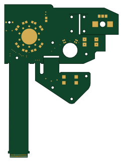
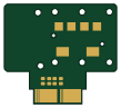
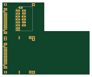
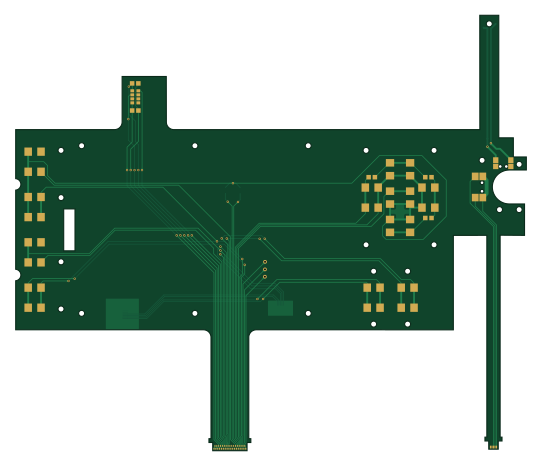
Back is an open source PCB design by cristibaluta, published on GitHub under the Custom license license. It is a 2-layer board measuring 135.2 × 115.3 mm, with 26 components from 23 distinct parts.
Other key parts include the 6N137. By type, the board carries 13 switches, 5 connectors, 4 capacitors, 3 resistors and 1 IC.
From the project
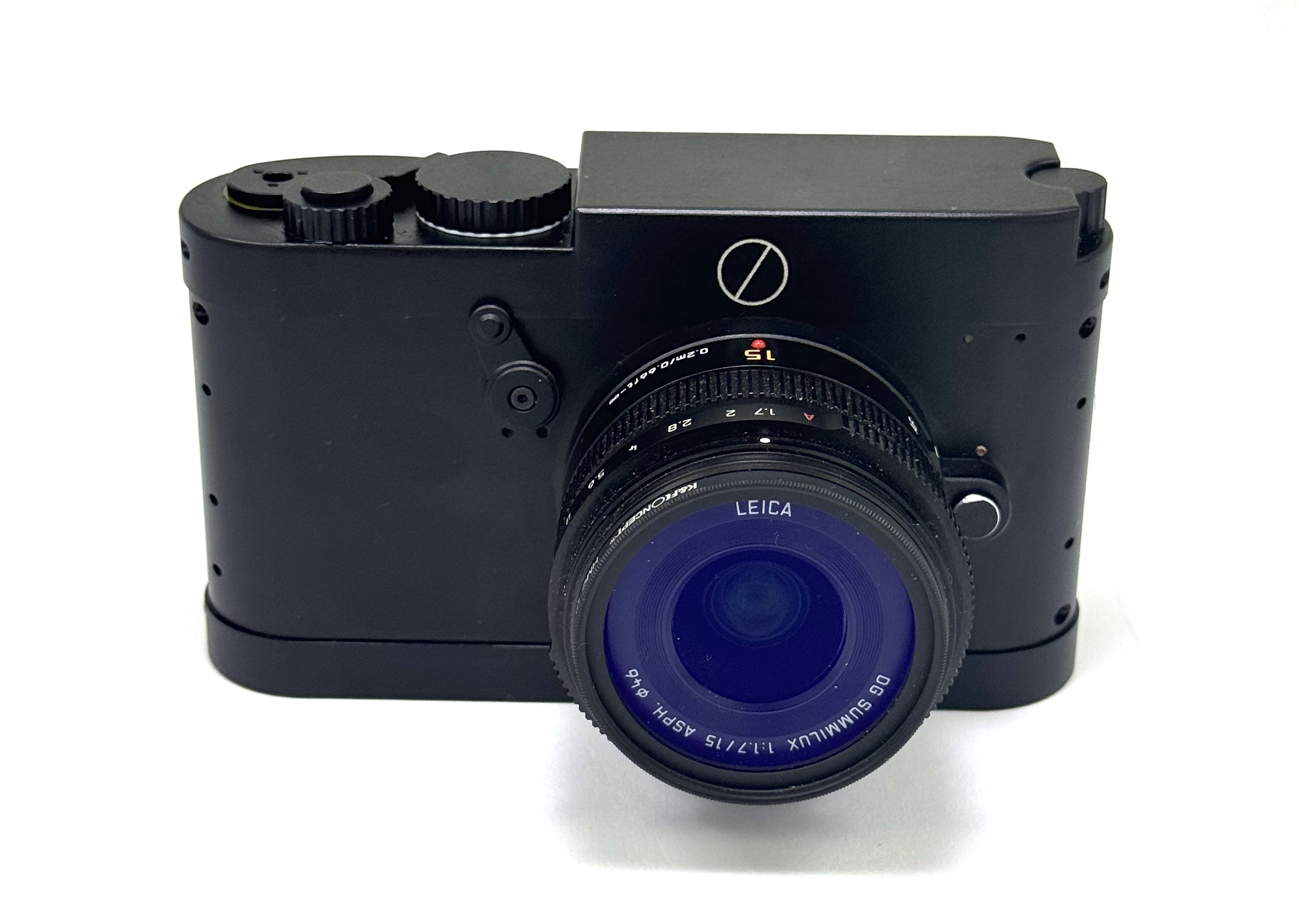
A complete hardware mod project that transforms the Panasonic Lumix G9ii into a Leica M-style camera
This project is an attempt to make a beautiful small camera from a Lumix G9II body. The camera is focused on street photography and has missing buttons and features.
If you are an expert in any relevant field and see mistakes you are welcome to open issues for discussion, my only qualification to do this is that I was into electronics a long time ago.
- /CADs/ – STEP files for CNC machining, including threads sheets - /FPCBs/ – Schematics and gerber files for the flex cables - /Datasheets/ – Some datasheets from used components - /BOM/ – List of extra items and purchase links
Main components on the Back
Back bill of materials (BOM)
26 components, 23 distinct parts.
| Qty | Part | Footprint | Refs |
|---|---|---|---|
| 1 | 6N137 | Optocoupler_EVF | U1 |
| 1 | To PCB | FPC-2Rows-35Pins-0.5mm | J1 |
| 1 | To Front | Connector-1Row-5Pins-0.40mm | J2 |
| 1 | Front | FPC-1Row-5Pins-0.40mm | J3 |
| 1 | From LCD | Connector-1Row-6Pins-0.40mm | J5 |
| 1 | To Right | Connector-Screw-2Pins | J6 |
| 1 | MENU/SET | Push_Button | SW1 |
| 1 | RIGHT | Push_Button | SW2 |
| 1 | DOWN | Push_Button | SW3 |
| 1 | LEFT | Push_Button | SW4 |
| 1 | UP | Push_Button | SW5 |
| 1 | BACK/DEL | Push_Button | SW6 |
| 1 | Q | Push_Button | SW7 |
| 1 | AF/ON | Push_Button | SW8 |
| 1 | DISP | Push_Button | SW9 |
| 1 | -+- | Push_Button | SW10 |
| 1 | PLAY | Push_Button | SW11 |
| 1 | S/C/M | Switch_Detection_Bidirectional | SW13 |
| 1 | ON/OFF | Switch_Detection | SW14 |
| 4 | C | R_0603 | C1, C2, C3, C4 |
Show 3 more
| Qty | Part | Footprint | Refs |
|---|---|---|---|
| 1 | 2.2K | R_0603 | R1 |
| 1 | 3.9K | R_0603 | R2 |
| 1 | 8K | R_0603 | R3 |
Back design files
The KiCad project lives in the cristibaluta/Leica-G9ii repository on GitHub; these links point at the commit this page was built from.
- LayoutFPCBs/Back/Back.kicad_pcb
- SchematicFPCBs/Back/Back.kicad_sch
Back: common questions
How big is the Back PCB?
The Back measures 135.2 × 115.3 mm, has 2 copper layers and is 1.6 mm thick.
How many components are on the Back?
26 components, from 23 distinct parts. The full bill of materials is listed on this page.
Where can I download the Back design files?
From the cristibaluta/Leica-G9ii repository on GitHub, which has the KiCad layout and the schematic; the links under Design files point to each one.
Can I use the Back design in my own project?
It is published under Custom license, which limits how it may be reused; read the license before building on it.