
USB Daughterboard

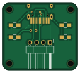
About the USB Daughterboard PCB
USB Daughterboard is an open source PCB design by Croktopus, published on GitHub under the GPL-3.0 license. It is a 2-layer board measuring 28 × 25.5 mm, with 6 components from 5 distinct parts.
It belongs with the keyboards and dev boards & breakouts designs in this gallery.
From the project
If you just want to have a CBC1 PCB printed, you'll want to take the gerbers.zip file to your PCB fab of choice (I recommend JLCPCB for the price), as well as the gerbers.zip in the daughterboard directory.
If you just want to have a CBC1 PCB printed, you'll want to take the gerbers.zip file to your PCB fab of choice (I recommend JLCPCB for the price), as well as the gerbers.zip in the daughterboard directory.
I've also got all the KiCad files in here if you want to play around with making your own modifications.
Once you have your PCB (unless you got it assembled for you), you get to do all the super fun SMT soldering! This is easily the worst part of the process IMO, but you can get through it in a few hours. If you haven't done this before, look up some youtube tutorials before you decide…
USB Daughterboard bill of materials (BOM)
6 components, 5 distinct parts — part numbers from the project's BOM.
| Qty | Part | Footprint | Refs |
|---|---|---|---|
| 1 | Conn_01x04 | Pin_Header_Angled_1x04_Pitch2.54mm_centered | J1 |
| 1 | 4.7n | C_0805_HandSoldering | C_SHIELD1 |
| 1 | 1M | R_0805_HandSoldering | R_SHIELD1 |
| 2 | 5.1K | R_0805_HandSoldering | R_USB1, R_USB2 |
| 1 | HRO-TYPE-C-31-M-12 | HRO-TYPE-C-31-M-12-HandSoldering | USB1 |
USB Daughterboard design files
The KiCad project lives in the Croktopus/Daishi repository on GitHub; these links point at the commit this page was built from.
USB Daughterboard: common questions
How big is the USB Daughterboard PCB?
The USB Daughterboard measures 28 × 25.5 mm, has 2 copper layers and is 1.6 mm thick.
How many components are on the USB Daughterboard?
6 components, from 5 distinct parts, with part numbers taken from the project's own BOM. The full bill of materials is listed on this page.
Where can I download the USB Daughterboard design files?
From the Croktopus/Daishi repository on GitHub, which has the KiCad layout and the BOM; the links under Design files point to each one.
Can I use the USB Daughterboard design in my own project?
Yes, under the terms of its GPL-3.0 license, which Croktopus chose for the repository.
More boards in Daishi
Similar boards
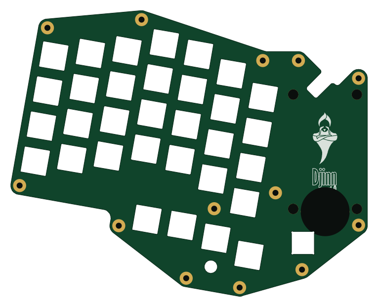
Board-DjinnPlate
tzarc
191 × 152.9 mm4 parts2LCERN-OHL-S-2.0988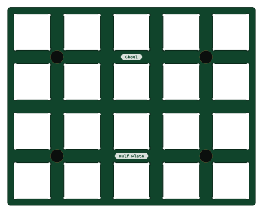
Half plate
95.3 × 76.2 mm24 parts2LCERN-OHL-S-2.0988
Hat
pa3gsb
65 × 56 mm81 parts2LNo license675
Radioberry juice
65 × 56 mm87 parts2LNo license675
Radioberry preamp
65 × 56 mm137 parts2LNo license675
Sram dev board
Wren6991
50 × 50 mm12 parts2LNo license508