
ElectricalPenetrationGraph

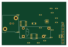
About the ElectricalPenetrationGraph PCB
ElectricalPenetrationGraph is an open source PCB design by DavidSternLab, published on GitHub. It is a 4-layer board measuring 60 × 40 mm, with 21 components from 8 distinct parts.
Other key parts include the HVQFN-16-1EP_3x3mm_P0.5mm_EP1.5x1.5mm, SOT-23-6 and SOIC-8_3.9x4.9mm_P1.27mm. By type, the board carries 6 capacitors, 2 ICs, 2 modules, 2 connectors and 1 relay.
From the project
An open, modern redesign of the Electrical Penetration Graph (EPG) recording rig — new hardware, firmware, and software — to replace the commercial Giga-8dd (EPG Systems EU / W.F. Tjallingii). Used to record stylet-penetration / feeding behavior of the pea aphid Acyrthosiphon pis
An open, modern redesign of the Electrical Penetration Graph (EPG) recording rig — new hardware, firmware, and software — to replace the commercial Giga-8dd (EPG Systems EU / W.F. Tjallingii). Used to record stylet-penetration / feeding behavior of the pea aphid Acyrthosiphon pisum.
1. Improve temporal resolution of sampling (original: 14-bit ADC @ 100 Hz default). 2. Reduce production cost. 3. Simplify construction. 4. Automate voltage-drift correction — the electrode-potential drift currently corrected by hand via the supplied voltage (Vs). An auto-detect/correct in firmware/software. 5.…
Main components on the ElectricalPenetrationGraph
ElectricalPenetrationGraph bill of materials (BOM)
21 components, 8 distinct parts.
| Qty | Part | Footprint | Refs |
|---|---|---|---|
| 1 | HVQFN-16-1EP_3x3mm_P0.5mm_EP1.5x1.5mm | HVQFN-16-1EP_3x3mm_P0.5mm_EP1.5x1.5mm | U3 |
| 1 | SOT-23-6 | SOT-23-6 | U4 |
| 2 | SOIC-8_3.9x4.9mm_P1.27mm | SOIC-8_3.9x4.9mm_P1.27mm | A1, A2 |
| 1 | BNC_Amphenol_031-5539_Vertical | BNC_Amphenol_031-5539_Vertical | J1 |
| 1 | PinHeader_1x08_P2.54mm_Vertical | PinHeader_1x08_P2.54mm_Vertical | J2 |
| 1 | Relay_1-Form-A_Schrack-RYII_RM5mm | Relay_1-Form-A_Schrack-RYII_RM5mm | K1 |
| 8 | R_0603_1608Metric | R_0603_1608Metric | RF1, RF2, RG1, RG2, RO1, RO2, RV1, RV2 |
| 6 | C_0603_1608Metric | C_0603_1608Metric | C1, C2, C3, C4, C5, C6 |
ElectricalPenetrationGraph design files
The KiCad project lives in the DavidSternLab/ElectricalPenetrationGraph repository on GitHub; these links point at the commit this page was built from.
ElectricalPenetrationGraph: common questions
How big is the ElectricalPenetrationGraph PCB?
The ElectricalPenetrationGraph measures 60 × 40 mm, has 4 copper layers and is 1.6 mm thick.
How many components are on the ElectricalPenetrationGraph?
21 components, from 8 distinct parts. The full bill of materials is listed on this page.
Where can I download the ElectricalPenetrationGraph design files?
From the DavidSternLab/ElectricalPenetrationGraph repository on GitHub, which has the KiCad layout; the links under Design files point to each one.
Can I use the ElectricalPenetrationGraph design in my own project?
The repository has no license, so all rights stay with DavidSternLab. Use it as a reference, and ask the author before reusing the design.