
INA219-Voltage Sensing

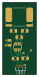
About the INA219-Voltage Sensing PCB
INA219-Voltage Sensing is an open source PCB design by Evans-Kwashie, published on GitHub under the CERN-OHL-S-2.0 license. It is a 4-layer board measuring 13 × 27.4 mm, with 7 components from 4 distinct parts.
By type, the board carries 4 resistors and 2 capacitors.
It belongs with the test & measurement designs in this gallery.
From the project
4-layer KiCad PCB for high-side current, bus-voltage and power monitoring with the TI INA219, using a 4-terminal Kelvin shunt, filtered sense inputs and an I2C interface.
A 4-layer PCB for high-side current and power sensing using the TI INA219, built as a self-directed mixed-signal design exercise. This board bridges an analog current-sense front end with a digital I2C interface, and was the first project in this series to require real attention to signal isolation and layer planning rather than single-layer routing.
The board measures current through a 4-terminal Kelvin-sense shunt resistor placed in the high-side power path (POWER in → shunt → LOAD out), and reports current, bus voltage, and power over I2C via the INA219. It's designed as an in-line…
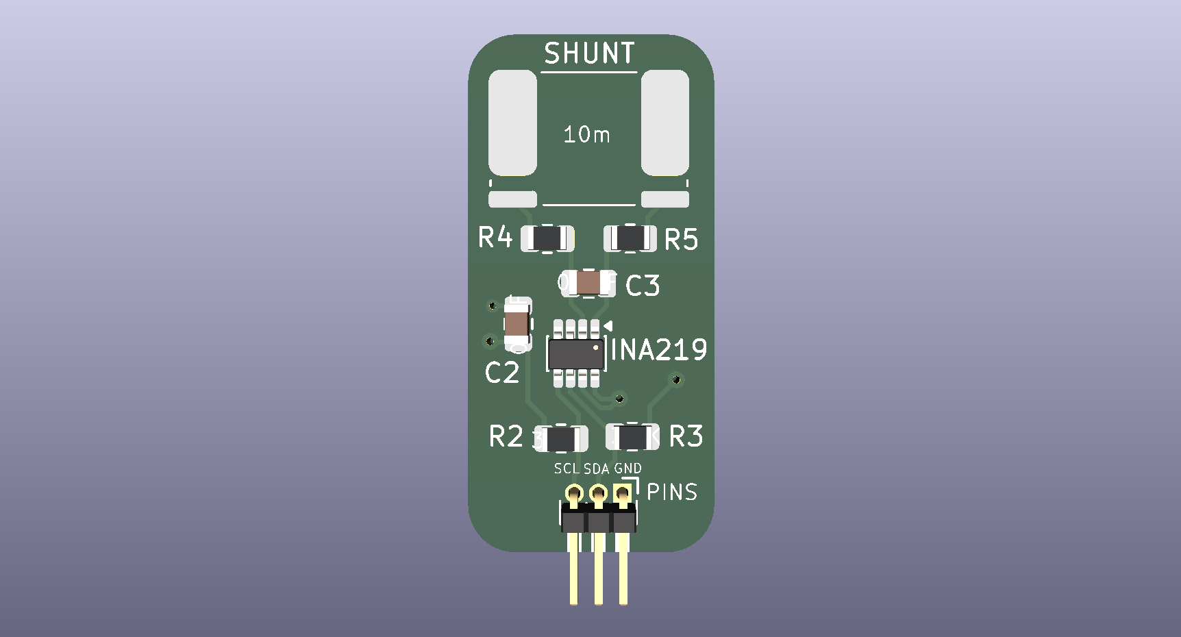
INA219-Voltage Sensing bill of materials (BOM)
7 components, 4 distinct parts.
| Qty | Part | Footprint | Refs |
|---|---|---|---|
| 1 | INA219AxDCN | SOT-23-8 | INA219 |
| 2 | 0.1uF | C_0805_2012Metric | C2, C3 |
| 2 | 3.3K | R_0805_2012Metric | R2, R3 |
| 2 | 10 | R_0805_2012Metric | R4, R5 |
INA219-Voltage Sensing design files
The KiCad project lives in the Evans-Kwashie/INA219-Voltage_Sensing_PCB repository on GitHub; these links point at the commit this page was built from.
- LayoutINA219.kicad_pcb
- SchematicINA219.kicad_sch
INA219-Voltage Sensing: common questions
How big is the INA219-Voltage Sensing PCB?
The INA219-Voltage Sensing measures 13 × 27.4 mm, has 4 copper layers and is 1.600198 mm thick.
How many components are on the INA219-Voltage Sensing?
7 components, from 4 distinct parts. The full bill of materials is listed on this page.
Where can I download the INA219-Voltage Sensing design files?
From the Evans-Kwashie/INA219-Voltage_Sensing_PCB repository on GitHub, which has the KiCad layout and the schematic; the links under Design files point to each one.
Can I use the INA219-Voltage Sensing design in my own project?
Yes, under the terms of its CERN-OHL-S-2.0 license, which Evans-Kwashie chose for the repository.
Similar boards
AnalyzerBoxPCB fork
gusmanb
52.7 × 47.9 mm54 parts4LGPL-3.05.0k
LevelShifter
28.3 × 39.8 mm21 parts2LGPL-3.05.0k
StackLink
52.3 × 10.5 mm5 parts2LGPL-3.05.0k
EleLab v2 Frontpanel a
Chrismettal
88 × 25 mm23 parts2LGPL-3.0528
EleLab v2 Bus150
150 × 50 mm37 parts2LGPL-3.0528
EleLab v2 PowerFeed
68 × 50 mm11 parts2LGPL-3.0528