
Project-LabEmbeddedDesign2

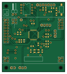
About the Project-LabEmbeddedDesign2 PCB
Project-LabEmbeddedDesign2 is an open source Silicon Labs PCB design by Fescron, published on GitHub under the GPL-3.0 license. It is a 2-layer board measuring 58.4 × 64.8 mm, with 37 components from 25 distinct parts.
Its main chip is the EFM32HG322F64, from the Silicon Labs family. Other key parts include the ADXL362-breakout. By type, the board carries 14 capacitors, 12 connectors, 6 resistors, 2 ICs, 2 crystals and 1 inductor.
It belongs with the sensors, rf & radio and iot & wireless designs in this gallery.
From the project
Project-LabEmbeddedDesign2
This repository contains the presentation, reports and code for the project constructed for Embedded System Design 2 - Lab.
- Reports and presentation - General important Doxygen documentation - Doxygen code documentation of individual files and methods - Code for the custom TTN decoder - Schematic of custom PCB - Schematic of DRAMCO LoRaWAN shield - Picture with PCB dimensions - The Things Network - Applications - Cayenne Dashboard
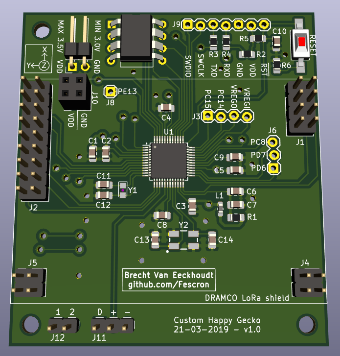
Main components on the Project-LabEmbeddedDesign2
Project-LabEmbeddedDesign2 bill of materials (BOM)
37 components, 25 distinct parts — part numbers from the project's BOM.
| Qty | Part | Footprint | Refs |
|---|---|---|---|
| 1 | EFM32HG322F64 EFM32HG322 Silicon Laboratories | TQFP-48_7x7mm_P0.5mm | U1 |
| 1 | ADXL362-breakout | DIP-8_W10.16mm | U2 |
| 1 | 32,768 kHz | Crystal_SMD_2012-2Pin_2.0x1.2mm_HandSoldering | Y1 |
| 1 | 24 MHz | CRYSTAL-SMD-5X3.2-4PAD | Y2 |
| 1 | Conn_02x04_Odd_Even | PinHeader_2x04_P2.54mm_Vertical | J1 |
| 1 | Conn_02x09_Odd_Even | PinHeader_2x09_P2.54mm_Vertical | J2 |
| 1 | Conn_01x04 | 1X04_LOCK | J3 |
| 2 | Conn_02x02_Odd_Even | PinHeader_2x02_P2.54mm_Vertical | J4, J5 |
| 2 | Conn_01x03 | 1X03_LOCK | J6, J11 |
| 1 | Conn_01x02 | PinHeader_1x02_P2.54mm_Horizontal | J7 |
| 1 | Conn_01x01 | 1X01 | J8 |
| 1 | Conn_01x07 | 1X07_LOCK | J9 |
| 1 | Conn_02x02_Odd_Even | PinSocket_2x02_P2.54mm_Vertical | J10 |
| 1 | Conn_01x02 | 1X02_LOCK | J12 |
| 1 | CBF102WB | L_0603_1608Metric_Pad1.05x0.95mm_HandSolder | L1 |
| 2 | 10 µF | C_0805_2012Metric_Pad1.15x1.40mm_HandSolder | C1, C6 |
| 5 | 100 nF | C_0805_2012Metric_Pad1.15x1.40mm_HandSolder | C2, C3, C4, C5, C10 |
| 2 | 10 nF | C_0805_2012Metric_Pad1.15x1.40mm_HandSolder | C7, C8 |
| 1 | 1 µF | C_0805_2012Metric_Pad1.15x1.40mm_HandSolder | C9 |
| 2 | 18 pF | C_0805_2012Metric_Pad1.15x1.40mm_HandSolder | C11, C12 |
Show 5 more
| Qty | Part | Footprint | Refs |
|---|---|---|---|
| 2 | 12 pF | C_0805_2012Metric_Pad1.15x1.40mm_HandSolder | C13, C14 |
| 1 | 1 Ω | R_0805_2012Metric_Pad1.15x1.40mm_HandSolder | R1 |
| 1 | 10 kΩ | R_0805_2012Metric_Pad1.15x1.40mm_HandSolder | R2 |
| 3 | 100 Ω | R_0805_2012Metric_Pad1.15x1.40mm_HandSolder | R3, R4, R6 |
| 1 | 1 kΩ | R_0805_2012Metric_Pad1.15x1.40mm_HandSolder | R5 |
Project-LabEmbeddedDesign2 design files
The KiCad project lives in the Fescron/Project-LabEmbeddedDesign2 repository on GitHub; these links point at the commit this page was built from.
Project-LabEmbeddedDesign2: common questions
What microcontroller does the Project-LabEmbeddedDesign2 use?
The Project-LabEmbeddedDesign2 is built around the EFM32HG322F64, from the Silicon Labs family.
How big is the Project-LabEmbeddedDesign2 PCB?
The Project-LabEmbeddedDesign2 measures 58.4 × 64.8 mm, has 2 copper layers and is 1.6 mm thick.
How many components are on the Project-LabEmbeddedDesign2?
37 components, from 25 distinct parts, with part numbers taken from the project's own BOM. The full bill of materials is listed on this page.
Where can I download the Project-LabEmbeddedDesign2 design files?
From the Fescron/Project-LabEmbeddedDesign2 repository on GitHub, which has the KiCad layout and the BOM; the links under Design files point to each one.
Can I use the Project-LabEmbeddedDesign2 design in my own project?
Yes, under the terms of its GPL-3.0 license, which Fescron chose for the repository.
Can I test firmware for the Project-LabEmbeddedDesign2 without the hardware?
Yes. HardLabs builds a simulation of the board from its netlist and BOM, so you can run and debug Silicon Labs firmware against it before you order a PCB.
Similar boards
 Silicon Labs
Tomu hardware
im-tomu
13 × 9.4 mm11 parts2LCC-BY-SA-4.0365 Silicon Labs
Ble soil moisture sensor
Miceuz
170 × 18 mm33 parts2LApache-2.033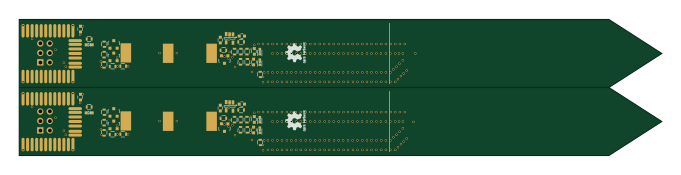 Silicon Labs
Ble soil moisture sensor pannel
170 × 36 mm29 parts2LApache-2.033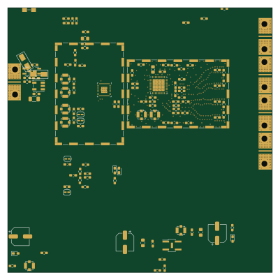 Silicon Labs
MWGEN-G1
MR-DOS
100 × 100 mm341 parts4LGPL-3.018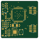 Silicon Labs
Efm32wg
dragonlock2
32 × 32 mm61 parts2LApache-2.013 Silicon Labs
DSMR-Splitter
basilfx
59.9 × 39.9 mm53 parts2LCC-BY-NC-4.07