
E nez

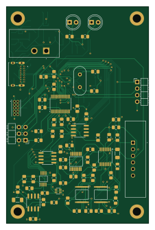
About the E nez PCB
E nez is an open source STM32 PCB design by gberthou, published on GitHub under the MIT license. It is a 4-layer board measuring 54.8 × 83.5 mm, with 104 components from 54 distinct parts.
Its main chip is the STM32C071CBT7, from the STM32 family. Other key parts include the LTC3440EMS#PBF, TCR2EF50,LM(CT, AD5270BRMZ-50, ADG1604BRUZ and OPA4387PWR. By type, the board carries 41 resistors, 39 capacitors, 14 ICs, 4 connectors, 3 diodes and 1 crystal.
From the project
Data acquisition platform | e-nez
Main components on the E nez
E nez bill of materials (BOM)
104 components, 54 distinct parts.
| Qty | Part | Footprint | Refs |
|---|---|---|---|
| 1 | LTC3440EMS#PBF | SOP50P490X110-10N | IC1 |
| 1 | TCR2EF50,LM(CT TCR2EF50,LM_CT | TCR2EF50LMCT | IC2 |
| 1 | AD5270BRMZ-50 | SOP50P490X110-10N | IC3 |
| 3 | ADG1604BRUZ | SOP65P640X120-14N | IC4, IC6, IC7 |
| 1 | STM32C071CBT7 | LQFP-48_7x7mm_P0.5mm | U1 |
| 1 | OPA4387PWR | TSSOP-14_4.4x5mm_P0.65mm | U2 |
| 1 | PCM1863QDBTRQ1 | TSSOP-30_4.4x7.8mm_P0.5mm | U3 |
| 2 | OPA2387DR | SOIC-8_3.9x4.9mm_P1.27mm | U4, U8 |
| 1 | MPX5050GP | MPX5050GP | U5 |
| 1 | MCP1725-3302E/SN | SOIC-8_3.9x4.9mm_P1.27mm | U6 |
| 1 | TLV9062IDR | SOIC-8_3.9x4.9mm_P1.27mm | U9 |
| 1 | ABL-12.288MHz-B1U | Crystal_HC49-U_Vertical | Y1 |
| 1 | USB4085-GF-A_REVA4 | GCT_USB4085-GF-A_REVA4 | J1 |
| 1 | FTSH-105-01-L-D FTSH-105-01-L-D-007-K | FTSH-105-XX-YYY-D | J2 |
| 1 | UART | PinHeader_1x04_P2.54mm_Horizontal | J3 |
| 1 | HTST-103-04-F-D-RA | PinHeader_2x03_P2.54mm_Horizontal | J4 |
| 1 | L101011MS02Q | L101011MS02Q | S1 |
| 2 | HLMP-K150 | LED_D5.0mm | D1, D2 |
| 1 | BAT54SDW | SOT-363_SC-70-6 | D3 |
| 1 | 10u | L_0805_2012Metric_Pad1.05x1.20mm_HandSolder | L1 |
Show 34 more
| Qty | Part | Footprint | Refs |
|---|---|---|---|
| 5 | 1u | C_0805_2012Metric_Pad1.18x1.45mm_HandSolder | C1, C22, C25, C28, C34 |
| 2 | 10n | C_0805_2012Metric_Pad1.18x1.45mm_HandSolder | C2, C20 |
| 1 | 1u | C_1206_3216Metric_Pad1.33x1.80mm_HandSolder | C3 |
| 1 | 10u | C_1206_3216Metric_Pad1.33x1.80mm_HandSolder | C4 |
| 14 | 100n | C_0805_2012Metric_Pad1.18x1.45mm_HandSolder | C5, C7, C14, C15, C21, C24, C26, C30 +6 |
| 2 | 470p | C_0805_2012Metric_Pad1.18x1.45mm_HandSolder | C6, C36 |
| 2 | 4.7u | C_0805_2012Metric_Pad1.18x1.45mm_HandSolder | C8, C18 |
| 2 | 26p; 08055A270FAT2A | C_0805_2012Metric_Pad1.18x1.45mm_HandSolder | C9, C10 |
| 5 | 10u | C_0805_2012Metric_Pad1.18x1.45mm_HandSolder | C11, C12, C13, C29, C32 |
| 1 | 2.2u | C_0805_2012Metric_Pad1.18x1.45mm_HandSolder | C16 |
| 1 | 22u | C_0805_2012Metric_Pad1.18x1.45mm_HandSolder | C19 |
| 2 | 1n | C_0805_2012Metric_Pad1.18x1.45mm_HandSolder | C23, C27 |
| 1 | 100n | R_0805_2012Metric_Pad1.20x1.40mm_HandSolder | C31 |
| 1 | 10k | R_0805_2012Metric | R1 |
| 1 | 20k | R_0805_2012Metric | R2 |
| 3 | 35k | R_0805_2012Metric_Pad1.20x1.40mm_HandSolder | R3, R13, R21 |
| 1 | 383k | R_0805_2012Metric_Pad1.20x1.40mm_HandSolder | R4 |
| 1 | 117k | R_0805_2012Metric_Pad1.20x1.40mm_HandSolder | R5 |
| 2 | 1.6k | R_0805_2012Metric_Pad1.20x1.40mm_HandSolder | R6, R7 |
| 4 | 100R | R_0805_2012Metric_Pad1.20x1.40mm_HandSolder | R8, R16, R17, R18 |
| 4 | 10k | R_0805_2012Metric_Pad1.20x1.40mm_HandSolder | R9, R14, R33, R40 |
| 2 | 15k | R_0805_2012Metric_Pad1.20x1.40mm_HandSolder | R10, R26 |
| 2 | 60k | R_0805_2012Metric_Pad1.20x1.40mm_HandSolder | R11, R19 |
| 1 | 25k | R_0805_2012Metric_Pad1.20x1.40mm_HandSolder | R12 |
| 1 | 1k | R_0805_2012Metric_Pad1.20x1.40mm_HandSolder | R15 |
| 1 | 30k | R_0805_2012Metric_Pad1.20x1.40mm_HandSolder | R20 |
| 1 | 40k | R_0805_2012Metric_Pad1.20x1.40mm_HandSolder | R22 |
| 4 | 5k | R_0805_2012Metric_Pad1.20x1.40mm_HandSolder | R23, R25, R28, R34 |
| 2 | 5.1k | R_0805_2012Metric_Pad1.20x1.40mm_HandSolder | R24, R29 |
| 1 | 20k | R_0805_2012Metric_Pad1.20x1.40mm_HandSolder | R27 |
| 4 | 33R | R_0805_2012Metric_Pad1.20x1.40mm_HandSolder | R30, R31, R41, R42 |
| 1 | 3.3k | R_0805_2012Metric_Pad1.20x1.40mm_HandSolder | R35 |
| 2 | 4.7k | R_0805_2012Metric_Pad1.20x1.40mm_HandSolder | R36, R39 |
| 2 | 2k | R_0805_2012Metric_Pad1.20x1.40mm_HandSolder | R37, R38 |
E nez design files
The KiCad project lives in the gberthou/e-nez repository on GitHub; these links point at the commit this page was built from.
- Layoutboard/e-nez.kicad_pcb
- Schematicboard/e-nez.kicad_sch
E nez: common questions
What microcontroller does the E nez use?
The E nez is built around the STM32C071CBT7, from the STM32 family.
How big is the E nez PCB?
The E nez measures 54.8 × 83.5 mm, has 4 copper layers and is 1.6 mm thick.
How many components are on the E nez?
104 components, from 54 distinct parts. The full bill of materials is listed on this page.
Where can I download the E nez design files?
From the gberthou/e-nez repository on GitHub, which has the KiCad layout and the schematic; the links under Design files point to each one.
Can I use the E nez design in my own project?
Yes, under the terms of its MIT license, which gberthou chose for the repository.
Can I test firmware for the E nez without the hardware?
Yes. HardLabs builds a simulation of the board from its netlist and BOM, so you can run and debug STM32 firmware against it before you order a PCB.
Similar boards
 STM32
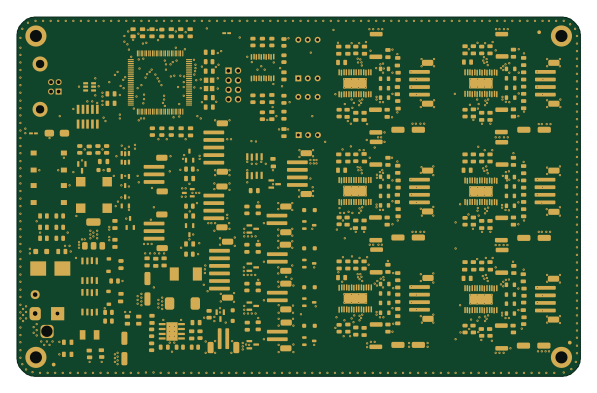
STM32LumenPnP Motherboard
opulo-inc
149 × 95 mm296 parts4LCC-BY-SA-4.03.7k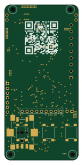 STM32
STM32AxxSolder
AxxAxx
39 × 82.5 mm122 parts2LGPL-3.01.7k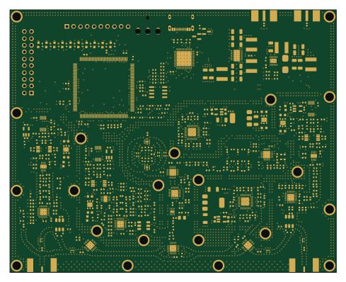 STM32
STM32LibreVNA
jankae
122 × 98 mm592 parts6LGPL-3.01.6k STM32
STM32AIOC
skuep
21 × 31.5 mm47 parts2LMIT1.4k STM32
STM32Ferris
pierrechevalier83
208.8 × 86.8 mm102 parts2LSHL-2.11.3k STM32
STM32176 pin board
rusefi
61.8 × 73.2 mm76 parts2LGPL-3.01.2k