
Kip

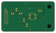
About the Kip PCB
Kip is an open source PCB design by GHawk1124, published on GitHub under the MIT license. It is a 2-layer board measuring 46 × 26 mm, with 8 components from 6 distinct parts.
Other key parts include the NE5534. By type, the board carries 4 capacitors, 2 resistors, 1 IC and 1 connector.
From the project
Engineering documents: Python in, vector PDF out.
Write engineering documents in Python. Build vector PDFs with unit-checked calculations, graph-paper layouts, tables, requirements and CAD drawings.
Edit doc.py directly. Put CAD in cad.py and optional reusable computations in analysis.py. rundocument(...) holds the title, running head and every other page setting. Inputs, requirements and references are workbooks under input/. Output goes in output/`.
Main components on the Kip
Kip bill of materials (BOM)
8 components, 6 distinct parts.
| Qty | Part | Footprint | Refs |
|---|---|---|---|
| 1 | NE5534 | SOIC-8_3.9x4.9mm_P1.27mm | U1 |
| 1 | Conn_01x05 | PinHeader_1x05_P2.54mm_Vertical | J1 |
| 1 | 22n | C_0805_2012Metric | C1 |
| 1 | 10n | C_0805_2012Metric | C2 |
| 2 | 100n | C_0805_2012Metric | C3, C4 |
| 2 | 10.7k | R_0805_2012Metric | R1, R2 |
Kip design files
The KiCad project lives in the GHawk1124/kip repository on GitHub; these links point at the commit this page was built from.
Kip: common questions
How big is the Kip PCB?
The Kip measures 46 × 26 mm, has 2 copper layers and is 1.6 mm thick.
How many components are on the Kip?
8 components, from 6 distinct parts. The full bill of materials is listed on this page.
Where can I download the Kip design files?
From the GHawk1124/kip repository on GitHub, which has the KiCad layout and the schematic; the links under Design files point to each one.
Can I use the Kip design in my own project?
Yes, under the terms of its MIT license, which GHawk1124 chose for the repository.