
M5stamp slic fxs

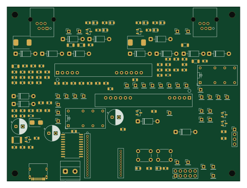
About the M5stamp slic fxs PCB
M5stamp slic fxs is an open source PCB design by GOROman, published on GitHub. It is a 2-layer board measuring 120 × 90 mm, with 154 components from 74 distinct parts.
Other key parts include the M5StampS3/S3A, 74HCT244, 1N4007, P3100SC and BZT03C82. By type, the board carries 38 resistors, 34 test points, 28 capacitors, 20 ICs, 9 diodes and 6 transistors.
From the project
Dual-port FXS line simulator / mini PBX board: M5StampS3 + 2x KS0835F (AG1171) SLIC modules for FAX/modem T.30 testing
ステータス: 基板 v3.4.1(配置版)が最新。配線済みデータは v3.4・未発注。2026-10-31 時点
2層・120×90mm・156部品の基板は、第7ラウンドの全数監査(物理干渉・シルク・ファームウェア整合・電気的妥当性・製造性・調達整合・極性)を通過した v3.4 を EasyEDA 上で配線完了しています(配線率 100%、未配線 0本、トラック 1,514 本・ビア 179 本、表裏 GND ベタあり。DRC の残件は配置由来のクリアランス指摘のみで、短絡・未接続はゼロ)。製造用 Gerber と EasyEDA 元データは gerber/ に同梱しています。
その後、発注前チェック(Issue #9・#12、いずれもクローズ済み)の是正を入れた v3.4.1 が現在の基板データ(kicad/SLIC2PORT-FXS.kicadpcb)です。v3.4 からの変更は3点のみ: SW2 を移動して SW1 とのパッド間隔 1.8mm を確保(従来は接触していた)、回線保護をメーカー図の GND 基準クランプに一致、RJ11 パッド幅を 1.13mm にして間隔・環状銅箔とも JLCPCB 基準内に是正。発注には v3.4.1 の EasyEDA 再取り込みと再配線が必要で、gerber/` の配線済みデータは v3.4…
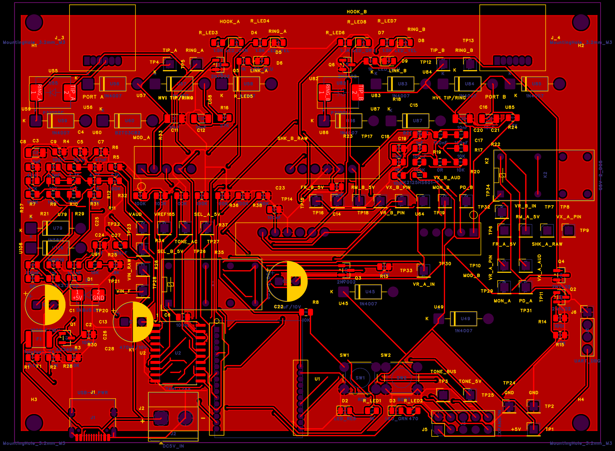
Main components on the M5stamp slic fxs
M5stamp slic fxs bill of materials (BOM)
154 components, 74 distinct parts.
| Qty | Part | Footprint | Refs |
|---|---|---|---|
| 1 | M5StampS3/S3A | Stamp-S3-Socket | U1 |
| 1 | 74HCT244 | SOIC-20W_7.5x12.8mm_P1.27mm | U2 |
| 10 | 1N4007 | D_DO-41_SOD81_P10.16mm_Horizontal | U45, U49, U56, U57, U58, U59, U83, U84 +2 |
| 2 | P3100SC | D_SMC | U55, U82 |
| 2 | BZT03C82 | D_DO-41_SOD81_P10.16mm_Horizontal | U60, U87 |
| 2 | BK2125HS601-T | L_0805_2012Metric | U64, U91 |
| 2 | 1N5819 | D_DO-41_SOD81_P10.16mm_Horizontal | U79, U106 |
| 1 | AO3401A | SOT-23 | Q1 |
| 5 | 2N7002 | SOT-23 | Q2, Q3, Q4, Q5, Q6 |
| 1 | USB-C_PWR | USB_C_Receptacle_HRO_TYPE-C-31-M-12 | J1 |
| 1 | DC5V_IN | TerminalBlock_Phoenix_MKDS-1,5-2_1x02_P5.00mm_Horizontal | J2 |
| 1 | EXPANSION | PinHeader_2x05_P2.54mm_Vertical | J5 |
| 1 | UART_DBG | PinHeader_1x04_P2.54mm_Vertical | J6 |
| 1 | Polyfuse_2A | Fuse_1812_4532Metric | F1 |
| 2 | RJ11_6P6C | RJ11_6P6C_TH | J_3, J_4 |
| 2 | G5V-2_DC5 | Relay_DPDT_Omron_G5V-2 | K1, K2 |
| 3 | 1K | R_0805_2012Metric | R_LED1, R_LED5, R_LED8 |
| 1 | 470 | R_0805_2012Metric | R_LED2 |
| 4 | 1.5K | R_0805_2012Metric | R_LED3, R_LED4, R_LED6, R_LED7 |
| 1 | RST | SW_PUSH_6mm | SW1 |
Show 54 more
| Qty | Part | Footprint | Refs |
|---|---|---|---|
| 1 | BOOT | SW_PUSH_6mm | SW2 |
| 1 | +5V | PinHeader_1x01_P2.54mm_Vertical | TP1 |
| 2 | GND | PinHeader_1x01_P2.54mm_Vertical | TP2, TP24 |
| 1 | TONE_BUS | PinHeader_1x01_P2.54mm_Vertical | TP3 |
| 1 | TIP_A | PinHeader_1x01_P2.54mm_Vertical | TP4 |
| 1 | RING_A | PinHeader_1x01_P2.54mm_Vertical | TP5 |
| 1 | FR_A_5V | PinHeader_1x01_P2.54mm_Vertical | TP6 |
| 1 | RM_A_5V | PinHeader_1x01_P2.54mm_Vertical | TP7 |
| 1 | SHK_A_RAW | PinHeader_1x01_P2.54mm_Vertical | TP8 |
| 1 | VX_A_PIN | PinHeader_1x01_P2.54mm_Vertical | TP9 |
| 1 | VR_A_PIN | PinHeader_1x01_P2.54mm_Vertical | TP10 |
| 1 | VX_A_AUD | PinHeader_1x01_P2.54mm_Vertical | TP11 |
| 1 | TIP_B | PinHeader_1x01_P2.54mm_Vertical | TP12 |
| 1 | RING_B | PinHeader_1x01_P2.54mm_Vertical | TP13 |
| 1 | FR_B_5V | PinHeader_1x01_P2.54mm_Vertical | TP14 |
| 1 | RM_B_5V | PinHeader_1x01_P2.54mm_Vertical | TP15 |
| 1 | SHK_B_RAW | PinHeader_1x01_P2.54mm_Vertical | TP16 |
| 1 | VX_B_PIN | PinHeader_1x01_P2.54mm_Vertical | TP17 |
| 1 | VR_B_PIN | PinHeader_1x01_P2.54mm_Vertical | TP18 |
| 1 | VX_B_AUD | PinHeader_1x01_P2.54mm_Vertical | TP19 |
| 1 | VIN_RAW | PinHeader_1x01_P2.54mm_Vertical | TP20 |
| 1 | VIN_F | PinHeader_1x01_P2.54mm_Vertical | TP21 |
| 1 | VAUD | PinHeader_1x01_P2.54mm_Vertical | TP22 |
| 1 | VREF165 | PinHeader_1x01_P2.54mm_Vertical | TP23 |
| 1 | TONE_5V | PinHeader_1x01_P2.54mm_Vertical | TP25 |
| 1 | TONE_AC | PinHeader_1x01_P2.54mm_Vertical | TP26 |
| 1 | SEL_A_5V | PinHeader_1x01_P2.54mm_Vertical | TP27 |
| 1 | SEL_B_5V | PinHeader_1x01_P2.54mm_Vertical | TP28 |
| 1 | MON_A | PinHeader_1x01_P2.54mm_Vertical | TP29 |
| 1 | MON_B | PinHeader_1x01_P2.54mm_Vertical | TP30 |
| 1 | PD_A | PinHeader_1x01_P2.54mm_Vertical | TP31 |
| 1 | PD_B | PinHeader_1x01_P2.54mm_Vertical | TP32 |
| 1 | VR_A_IN | PinHeader_1x01_P2.54mm_Vertical | TP33 |
| 1 | VR_B_IN | PinHeader_1x01_P2.54mm_Vertical | TP34 |
| 1 | SMBJ5.0A | D_SMB | D1 |
| 1 | LED_RED | LED_0805_2012Metric | D2 |
| 3 | LED_GRN | LED_0805_2012Metric | D3, D4, D7 |
| 2 | LED_YEL | LED_0805_2012Metric | D5, D8 |
| 2 | LED_BLU | LED_0805_2012Metric | D6, D9 |
| 1 | 1000uF/10V | CP_Radial_D8.0mm_P3.50mm | C1 |
| 14 | 100nF | C_0805_2012Metric | C2, C4, C5, C6, C9, C10, C14, C16 +6 |
| 1 | 10uF | C_1206_3216Metric | C3 |
| 2 | 47nF | C_0805_2012Metric | C7, C8 |
| 4 | 10nF | C_1206_3216Metric | C11, C12, C20, C21 |
| 2 | 470uF/10V | CP_Radial_D8.0mm_P3.50mm | C13, C22 |
| 4 | 1nF | C_0805_2012Metric | C15, C18, C24, C27 |
| 2 | 5.1K | R_0805_2012Metric | R1, R2 |
| 18 | 100K | R_0805_2012Metric | R3, R12, R13, R14, R15, R19, R21, R23 +10 |
| 2 | 4.7K | R_0805_2012Metric | R4, R5 |
| 3 | 47K | R_0805_2012Metric | R6, R7, R11 |
| 7 | 10K | R_0805_2012Metric | R8, R9, R10, R17, R22, R25, R30 |
| 2 | 27K | R_0805_2012Metric | R16, R24 |
| 2 | 18K | R_0805_2012Metric | R18, R26 |
| 2 | 0R | R_0805_2012Metric | R20, R28 |
M5stamp slic fxs design files
The KiCad project lives in the GOROman/m5stamp-slic-fxs repository on GitHub; these links point at the commit this page was built from.
M5stamp slic fxs: common questions
How big is the M5stamp slic fxs PCB?
The M5stamp slic fxs measures 120 × 90 mm, has 2 copper layers and is 1.6 mm thick.
How many components are on the M5stamp slic fxs?
154 components, from 74 distinct parts. The full bill of materials is listed on this page.
Where can I download the M5stamp slic fxs design files?
From the GOROman/m5stamp-slic-fxs repository on GitHub, which has the KiCad layout; the links under Design files point to each one.
Can I use the M5stamp slic fxs design in my own project?
The repository has no license, so all rights stay with GOROman. Use it as a reference, and ask the author before reusing the design.
Earlier revisions in the repo: SLIC2PORT-FXS