
Input PCB V5

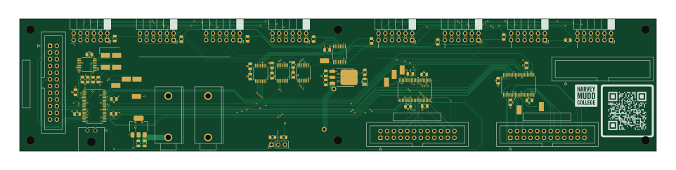
About the Input PCB V5
Input PCB V5 is an open source PCB design by hrl-labs-clinic-24-25, published on GitHub. It is a 4-layer board measuring 240 × 50 mm, with 79 components from 19 distinct parts.
Other key parts include the C2862419, C151391, C347220, C352826 and C2938871. By type, the board carries 24 capacitors, 15 connectors, 15 resistors, 14 transformers, 10 ICs and 1 diode.
From the project
Mostly arduino code for simulating the output of the FPGA. Mainly used to control DACs with SPI.
Main components on the Input PCB V5
Input PCB V5 bill of materials (BOM)
79 components, 19 distinct parts — part numbers from the project's BOM.
| Qty | Part | Footprint | Refs |
|---|---|---|---|
| 3 | C2862419 SN74AUC16244DGGR | DGG48 | U1, U2, U5 |
| 1 | C151391 AZ1084CD-3.3TRG1 | TO-252-3_TabPin2 | U3 |
| 1 | C347220 AMS1117-1.8 | SOT-223-3_TabPin2 | U4 |
| 2 | C352826 CD74HC4051PWR | PW16 | U6, U10 |
| 3 | C2938871 TXU0104PWR | TSSOP_0104PWR_TEX | U7, U8, U9 |
| 1 | C5360899 Conn_01x03 | PinHeader_1x03_P2.54mm_Vertical | J1 |
| 3 | C7501246 Conn_02x12_Odd_Even | IDC-Header_2x12_P2.54mm_Vertical | J2, J4, J7 |
| 1 | C192562 436500200 | CONN_SD-43650-001_02_MOL | J3 |
| 1 | C7437321 Red Banana | CONN-TH_24.243.2_Better_Silkscreen | J5 |
| 1 | C7437322 Black Banana | CONN-TH_24.243.2_Better_Silkscreen | J6 |
| 8 | C2897426 Conn_02x06_Odd_Even | PinSocket_2x06_P2.54mm_Horizontal | J8, J9, J10, J11, J12, J13, J14, J15 |
| 13 | C3345122 TestPoint | HARWIN_S1751-46R | T1, T2, T3, T4, T5, T6, T7, T8 +5 |
| 1 | TestPoint | HARWIN_S1751-46R | T14 |
| 1 | C7466711 HSMA-C170 | LED_0805_2012Metric | D1 |
| 20 | 0.1uF | C_0805_2012Metric | C1, C2, C3, C4, C9, C10, C11, C12 +12 |
| 2 | 10uF | C_0805_2012Metric | C5, C6 |
| 2 | 22uF | C_0805_2012Metric | C7, C8 |
| 14 | 10k | R_0805_2012Metric | R1, R2, R4, R5, R6, R7, R8, R9 +6 |
| 1 | 2.2k | R_0805_2012Metric | R3 |
Input PCB V5 design files
The KiCad project lives in the hrl-labs-clinic-24-25/hardware-prototyping repository on GitHub; these links point at the commit this page was built from.
Input PCB V5: common questions
How big is the Input PCB V5?
The Input PCB V5 measures 240 × 50 mm, has 4 copper layers and is 1.6 mm thick.
How many components are on the Input PCB V5?
79 components, from 19 distinct parts, with part numbers taken from the project's own BOM. The full bill of materials is listed on this page.
Where can I download the Input PCB V5 design files?
From the hrl-labs-clinic-24-25/hardware-prototyping repository on GitHub, which has the KiCad layout, the schematic and the BOM; the links under Design files point to each one.
Can I use the Input PCB V5 design in my own project?
The repository has no license, so all rights stay with hrl-labs-clinic-24-25. Use it as a reference, and ask the author before reusing the design.
More boards in hardware-prototyping
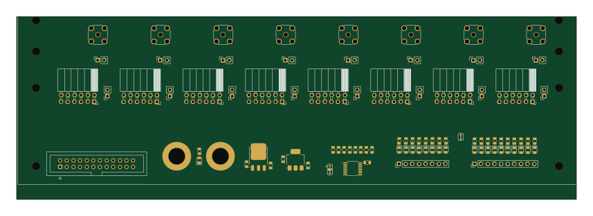
Mux2
214 × 70 mm91 parts2LNo license1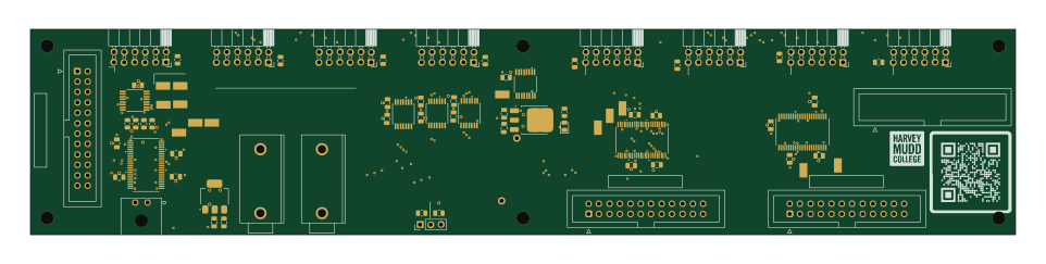
Input pcb2
240 × 50 mm78 parts4LNo license1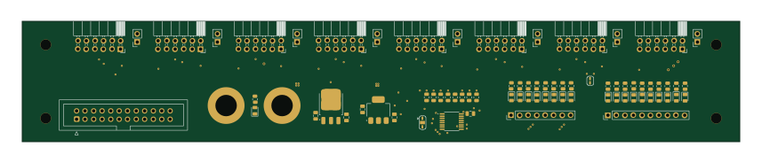
Mux
214 × 36 mm73 parts2LNo license1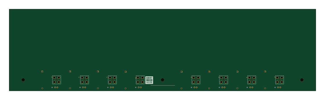
Output Board
279.4 × 75 mm48 parts2LNo license1
SMA
214 × 26 mm18 parts2LNo license1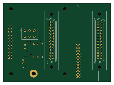
Coupler board
96 × 70 mm9 parts2LNo license1
Earlier revisions in the repo: Input_PCB_V4, Input_PCB_V3