
Flash breakout


About the Flash breakout
Flash breakout is an open source PCB design by hulkco, published on GitHub. It is a 2-layer board measuring 11.4 × 12.7 mm, with 3 components from 3 distinct parts.
Other key parts include the AP2112-3.3. By type, the board carries 1 IC, 1 connector and 1 resistor.
It belongs with the wearables and dev boards & breakouts designs in this gallery.
From the project
Upload "Oshwi" Badge for OshwDem 2017 a Coruña
Main components on the Flash breakout
Flash breakout bill of materials (BOM)
3 components, 3 distinct parts — part numbers from the project's BOM.
| Qty | Part | Footprint | Refs |
|---|---|---|---|
| 1 | AP2112-3.3 SPIFLASH_SOIC8208MIL | SOIC-8_3.9x4.9mm_P1.27mm | U1 |
| 1 | Conn_01x05 | PinSocket_1x05_P2.54mm_Vertical | J1 |
| 1 | 100K R | R_0805_2012Metric_Pad1.15x1.40mm_HandSolder | R1 |
Flash breakout design files
The KiCad project lives in the hulkco/oshwi repository on GitHub; these links point at the commit this page was built from.
Flash breakout: common questions
How big is the Flash breakout?
The Flash breakout measures 11.4 × 12.7 mm, has 2 copper layers and is 1.6 mm thick.
How many components are on the Flash breakout?
3 components, from 3 distinct parts, with part numbers taken from the project's own BOM. The full bill of materials is listed on this page.
Where can I download the Flash breakout design files?
From the hulkco/oshwi repository on GitHub, which has the KiCad layout and the BOM; the links under Design files point to each one.
Can I use the Flash breakout design in my own project?
The repository has no license, so all rights stay with hulkco. Use it as a reference, and ask the author before reusing the design.
More boards in oshwi
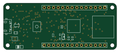 Microchip SAM
MKRZero V5.0
61.5 × 25 mm91 partsNo license15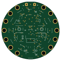 Microchip SAM
Adafruit Circuit Playground Express
50.8 × 50.6 mm78 partsNo license15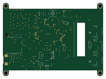 Microchip SAM
Adafruit PyPortal
88.3 × 64.5 mm75 partsNo license15 ESP8266
Project Title
74.7 × 96.8 mm51 parts2LNo license15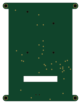
Adafruit 3.5in 480x320 FeatherWing
66 × 85.3 mm33 partsNo license15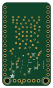 ESP32
Adafruit ESP32 Huzzah Breakout
25.4 × 43.7 mm23 partsNo license15 ESP8266
Oshwi ESP8266 LORA
83.9 × 108.8 mm22 partsNo license15 ESP32
Oshwi ESP32
83.9 × 108.8 mm21 parts2LNo license15 AVR/Arduino
SMD
34.7 × 21.5 mm20 partsNo license15
Similar boards
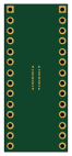
BM28B0.6-24DSBreakout
scottbez1
15.2 × 35.6 mm3 parts2LApache-2.022.2k
LevelShifterBreakout
15.2 × 20.3 mm5 parts2LApache-2.022.2k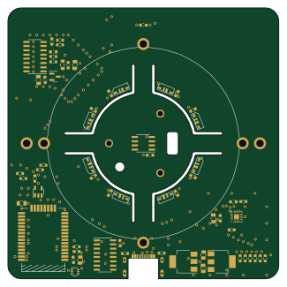
View base
81.2 × 81.2 mm81 parts2LApache-2.022.2k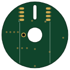
View screen
35 × 35 mm12 parts2LApache-2.022.2k
ChainlinkBase
98.4 × 190.5 mm119 parts2LApache-2.04.2k
ChainlinkDriverTester
198.1 × 95.3 mm123 parts2LApache-2.04.2k