
Kicad projects

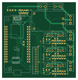
About the Kicad projects PCB
Kicad projects is an open source PCB design by jibonaronno, published on GitHub under the CC0-1.0 license. It is a 2-layer board measuring 74.6 × 76.8 mm, with 47 components from 13 distinct parts.
Other key parts include the TLP291. By type, the board carries 18 resistors, 10 diodes, 6 transistors, 6 capacitors, 4 ICs and 1 connector.
From the project
Practically there are 2 types of dimmer.
Practically there are 2 types of dimmer.
Based on the swithing time position after zero cross detection.
Here is a simple concept of raising and trailing edge switching.
This project focused on trailing edge dimmer construction.
Here it stores energy in C5 and C6 from power line ACL and ACN. From the perspective it only uses positive cycle of the phase to store energy. Turning on the mosfet is occured by Opto U2, and turning off is happened by R14 (10k) . So this dimmer is not suitable for more than 200W.
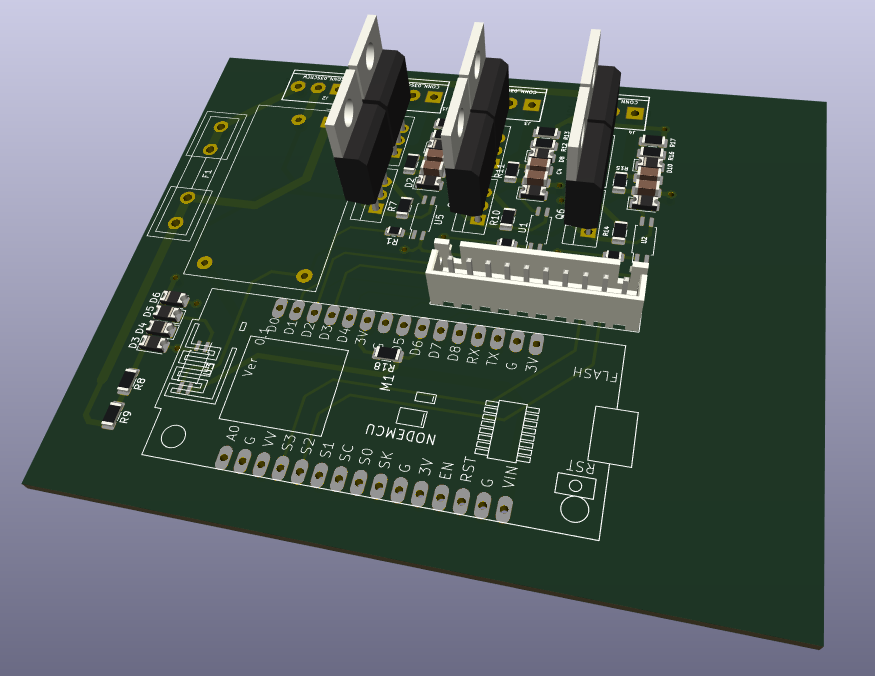
Main components on the Kicad projects
Kicad projects bill of materials (BOM)
47 components, 13 distinct parts — part numbers from the project's BOM.
| Qty | Part | Footprint | Refs |
|---|---|---|---|
| 4 | TLP291 | SOIC-4_4.55x2.6mm_P1.27mm | U1, U2, U3, U5 |
| 6 | IRF740 | TO-220-3_Vertical | Q1, Q2, Q3, Q4, Q5, Q6 |
| 1 | CONN_01X10 Conn_01x10 | JST_XH_B10B-XH-A_1x10_P2.50mm_Vertical | J5 |
| 1 | Fuse 5A | Fuseholder5x20_horiz_open_inline_Type-I | F1 |
| 1 | HLK-PM01 | Converter_ACDC_HiLink_HLK-PMxx | PS1 |
| 7 | 4007 | D_1206_3216Metric | D1, D3, D4, D5, D6, D8, D10 |
| 3 | 12V | D_1206_3216Metric | D2, D7, D9 |
| 6 | 10 | C_1206_3216Metric | C1, C2, C3, C4, C5, C6 |
| 3 | 220E | R_0805_2012Metric | R1, R2, R3 |
| 6 | 15K | R_1206_3216Metric | R4, R5, R12, R13, R16, R17 |
| 3 | 100E | R_1206_3216Metric | R6, R11, R15 |
| 4 | 10K | R_1206_3216Metric | R7, R10, R14, R18 |
| 2 | 33K | R_1206_3216Metric | R8, R9 |
Kicad projects design files
The KiCad project lives in the jibonaronno/kicad_projects repository on GitHub; these links point at the commit this page was built from.
Kicad projects: common questions
How big is the Kicad projects PCB?
The Kicad projects measures 74.6 × 76.8 mm, has 2 copper layers and is 1.6 mm thick.
How many components are on the Kicad projects?
47 components, from 13 distinct parts, with part numbers taken from the project's own BOM. The full bill of materials is listed on this page.
Where can I download the Kicad projects design files?
From the jibonaronno/kicad_projects repository on GitHub, which has the KiCad layout, the schematic and the BOM; the links under Design files point to each one.
Can I use the Kicad projects design in my own project?
Yes, under the terms of its CC0-1.0 license, which jibonaronno chose for the repository.