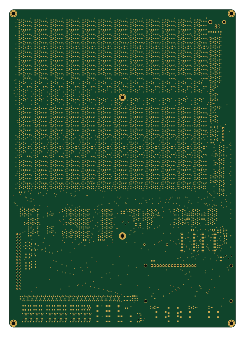
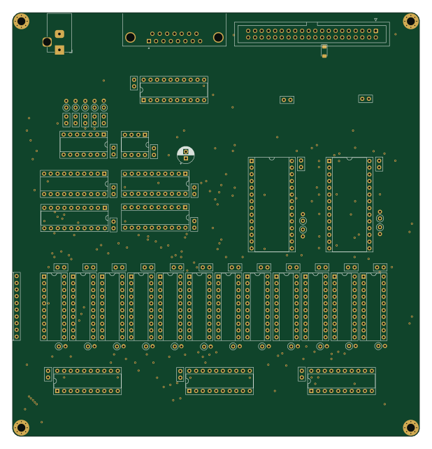
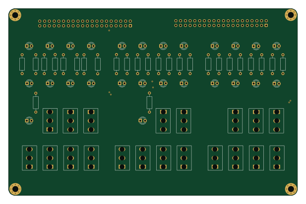
Terminal

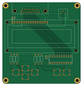
About the Terminal PCB
Terminal is an open source PCB design by joewing, published on GitHub. It is a 2-layer board measuring 85 × 89.2 mm, with 17 components from 11 distinct parts.
Other key parts include the 540. By type, the board carries 6 switches, 6 resistors, 2 capacitors and 1 IC.
From the project
12-bit single-board discrete transistor computer
Hardware for the Q2 12-bit computer made from programmable logic devices. Compared to the original Q2, the Q2A should be easier to have fabricated (it uses through-hole components making it easy to hand assemble). In addition, the Q2A has a faster clock and a nicer enclosure.
Note that the current iteration of the Q2A does not support the memory extension device or I2C.
Main components on the Terminal
Terminal bill of materials (BOM)
17 components, 11 distinct parts.
| Qty | Part | Footprint | Refs |
|---|---|---|---|
| 1 | 540 | DIP-20_W7.62mm_Socket | U1 |
| 1 | WC1602A | WC1602A | DS1 |
| 1 | 10k | Potentiometer_Bourns_3386P_Vertical | RV1 |
| 1 | A | SW_PUSH_6mm | SW1 |
| 1 | B | SW_PUSH_6mm | SW2 |
| 1 | UP | SW_PUSH_6mm | SW3 |
| 1 | DOWN | SW_PUSH_6mm | SW4 |
| 1 | LEFT | SW_PUSH_6mm | SW5 |
| 1 | RIGHT | SW_PUSH_6mm | SW6 |
| 2 | 0.1u | C_Disc_D3.4mm_W2.1mm_P2.50mm | C1, C2 |
| 6 | 10k | R_Axial_DIN0207_L6.3mm_D2.5mm_P10.16mm_Horizontal | R1, R2, R3, R4, R5, R6 |
Terminal design files
The KiCad project lives in the joewing/q2 repository on GitHub; these links point at the commit this page was built from.
Terminal: common questions
How big is the Terminal PCB?
The Terminal measures 85 × 89.2 mm, has 2 copper layers and is 1.6 mm thick.
How many components are on the Terminal?
17 components, from 11 distinct parts. The full bill of materials is listed on this page.
Where can I download the Terminal design files?
From the joewing/q2 repository on GitHub, which has the KiCad layout and the schematic; the links under Design files point to each one.
Can I use the Terminal design in my own project?
The repository has no license, so all rights stay with joewing. Use it as a reference, and ask the author before reusing the design.