
Pcb agent workflow

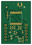
About the Pcb agent workflow
Pcb agent workflow is an open source PCB design by John-owo, published on GitHub under the MIT license. It is a 4-layer board measuring 25 × 36.5 mm, with 19 components from 14 distinct parts.
Other key parts include the MAX-M10S-00B. By type, the board carries 8 resistors, 3 connectors, 3 diodes, 3 capacitors, 1 IC and 1 transistor.
From the project
用 Claude Code/Codex 搭配 KiCad 10 設計 PCB、交 JLCPCB 製造的工作流程:流程文件、專案範本、JLC 客服溝通 skill、生產稿比對腳本與範例設計
以 u-blox MAX-M10S 為核心的小型 GNSS 轉接板,接被動式天線,供麵包板或主控板以 UART/I2C 使用。原生設計為 KiCad 10,發行日期 2026-09-21。
- 尺寸 25.0 × 36.5 mm,4 層,板厚 1.6 mm,表面處理 OSP,疊構按 JLC04161H-7628 設定。 - U1:MAX-M10S-00B,使用預設低增益內建 LNA。 - J1:I-PEX MHF I(20279-001E-03)接被動式 50 Ω 天線,不供天線電源。D1 為天線端 ESD 保護。 - J2、J3:兩支 1×6、2.54 mm 排針,從板底插入,兩排間距 17.78 mm。 - TX/RX/PPS 串 33 Ω,I2C 有 4.7 kΩ 上拉,電源 LED,PPS LED 經 BSS138 緩衝。另有 5 個測試焊盤(TP1、TP2、TP4–TP6)。 - 無 RTC 備援電源:U1 pin 6(V_BCKP)刻意不接,板上沒有電池或超級電容。 - 原理圖註記:UART 9600 8N1,I2C 位址 0x42。
Main components on the Pcb agent workflow
Pcb agent workflow bill of materials (BOM)
19 components, 14 distinct parts — part numbers from the project's BOM.
| Qty | Part | Footprint | Refs |
|---|---|---|---|
| 1 | MAX-M10S-00B u-blox | MAX_M10S | U1 |
| 1 | BSS138 onsemi | SOT23 | Q1 |
| 1 | 20279-001E-03 MHF I PASSIVE ANT I-PEX | MHF_I | J1 |
| 1 | HX PH254-01-06-Z-L11.5 POWER / UART / PPS hanxia | Header_1x06 | J2 |
| 1 | HX PH254-01-06-Z-L11.5 I2C / CONTROL hanxia | Header_1x06 | J3 |
| 1 | PESD3V3Z1BSFYL Nexperia | PESD3V3C1BSF | D1 |
| 1 | 19-21/G6C-FM1N2B/4T PWR green Everlight | LED_0603 | D2 |
| 1 | 19-21/G6C-FM1N2B/4T PPS green Everlight | LED_0603 | D3 |
| 2 | CC0603KRX7R9BB104 100nF YAGEO | C_0603 | C1, C2 |
| 1 | CL10A106KP8NNNC 10uF Samsung Electro-Mechanics | C_0603 | C3 |
| 3 | 0603WAF330JT5E 33R UNI-ROYAL | R_0603 | R1, R2, R3 |
| 2 | 0603WAF4701T5E 4.7k UNI-ROYAL | R_0603 | R4, R5 |
| 2 | 0603WAF2201T5E 2.2k UNI-ROYAL | R_0603 | R6, R7 |
| 1 | 0603WAF1004T5E 1M UNI-ROYAL | R_0603 | R8 |
Pcb agent workflow design files
The KiCad project lives in the John-owo/pcb-agent-workflow repository on GitHub; these links point at the commit this page was built from.
Pcb agent workflow: common questions
How big is the Pcb agent workflow?
The Pcb agent workflow measures 25 × 36.5 mm, has 4 copper layers and is 1.6 mm thick.
How many components are on the Pcb agent workflow?
19 components, from 14 distinct parts, with part numbers taken from the project's own BOM. The full bill of materials is listed on this page.
Where can I download the Pcb agent workflow design files?
From the John-owo/pcb-agent-workflow repository on GitHub, which has the KiCad layout, the schematic and the BOM; the links under Design files point to each one.
Can I use the Pcb agent workflow design in my own project?
Yes, under the terms of its MIT license, which John-owo chose for the repository.