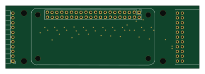
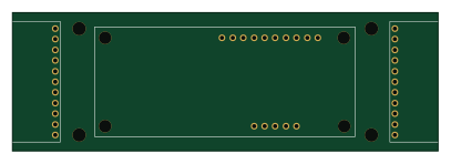
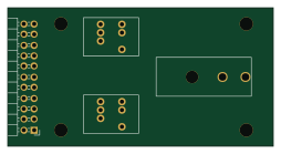
Optical digitizer

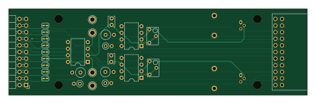
About the Optical digitizer PCB
Optical digitizer is an open source PCB design by jrleeman, published on GitHub. It is a 4-layer board measuring 114.3 × 33 mm, with 21 components from 10 distinct parts.
Other key parts include the OPA350 and MCP3202. By type, the board carries 8 capacitors, 4 test points, 3 ICs, 2 connectors and 2 diodes.
From the project
Optical Fiber Michelson Interrogator (OFMI) designed for geophysical applications by Dr. Scott DeWolf
Main components on the Optical digitizer
Optical digitizer bill of materials (BOM)
21 components, 10 distinct parts.
| Qty | Part | Footprint | Refs |
|---|---|---|---|
| 2 | OPA350 | DIP-8_W7.62mm | U1, U2 |
| 1 | MCP3202 | DIP-8_W7.62mm | U3 |
| 1 | Female Input Connector | Pin_Header_Angled_2x11_Pitch2.54mm | J1 |
| 1 | Male Output Connector | SAMTEC-SSW-111-02-X-D-RA | J2 |
| 2 | 100k | 3266W | RV1, RV2 |
| 4 | TestPoint | 5006_TestPoint | TP1, TP2, TP3, TP4 |
| 2 | PhotoDiode | PhotoDiode | D1, D2 |
| 3 | 0.1uF | 2.54x4.32CAP | C1, C3, C7 |
| 3 | 1uF | 3.81x10.16CAP | C2, C4, C8 |
| 2 | 1pF | C_Rect_L4.0mm_W2.5mm_P2.50mm | C5, C6 |
Optical digitizer design files
The KiCad project lives in the jrleeman/Clemson_OFMI repository on GitHub; these links point at the commit this page was built from.
Optical digitizer: common questions
How big is the Optical digitizer PCB?
The Optical digitizer measures 114.3 × 33 mm, has 4 copper layers and is 1.6 mm thick.
How many components are on the Optical digitizer?
21 components, from 10 distinct parts. The full bill of materials is listed on this page.
Where can I download the Optical digitizer design files?
From the jrleeman/Clemson_OFMI repository on GitHub, which has the KiCad layout; the links under Design files point to each one.
Can I use the Optical digitizer design in my own project?
The repository has no license, so all rights stay with jrleeman. Use it as a reference, and ask the author before reusing the design.