
Openclack

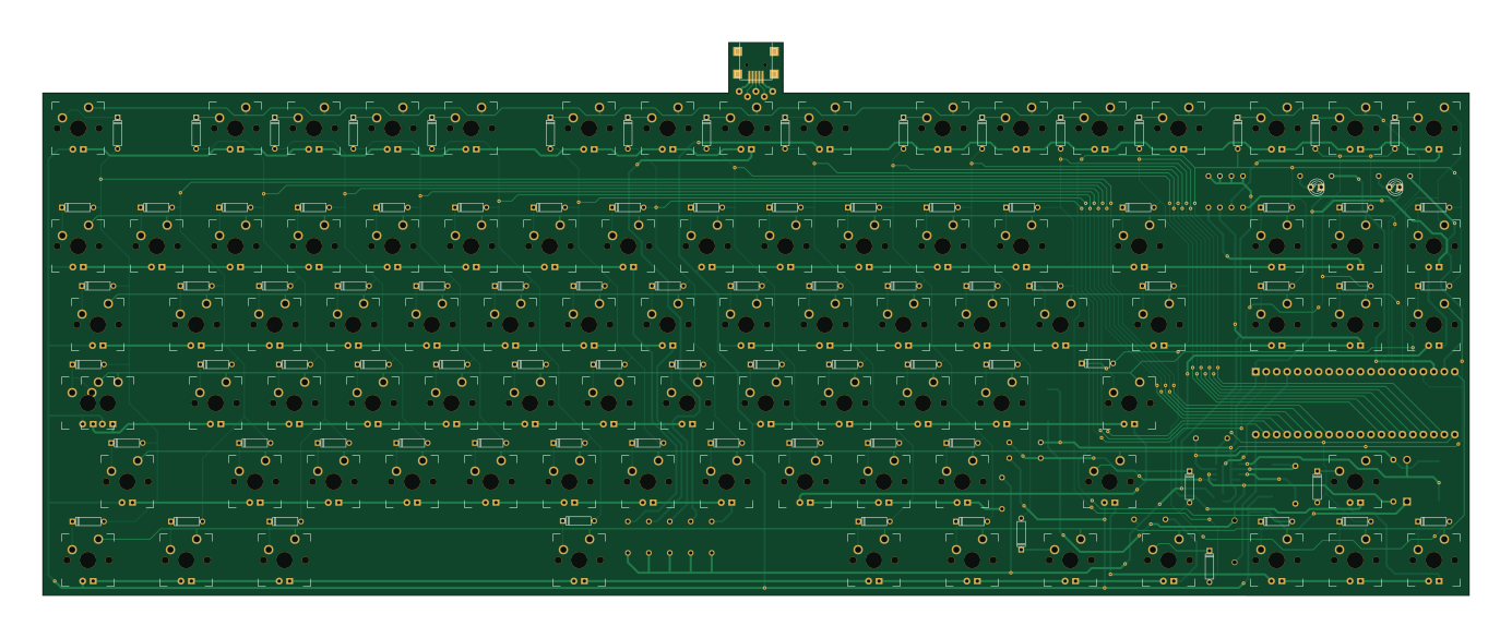
About the Openclack PCB
Openclack is an open source NXP PCB design by jtryon, published on GitHub. It is a 2-layer board measuring 345.7 × 134.1 mm, with 204 components from 107 distinct parts.
Its main chip is the TEENSYPP2, from the NXP family. Other key parts include the USB-MINI-B_EXT. By type, the board carries 89 diodes, 87 switches, 11 resistors, 2 ICs, 1 transistor and 1 connector.
It belongs with the keyboards designs in this gallery.
From the project
OpenClack
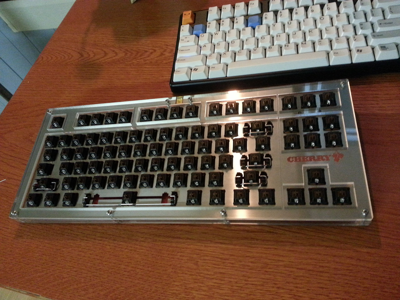
Main components on the Openclack
Openclack bill of materials (BOM)
204 components, 107 distinct parts.
| Qty | Part | Footprint | Refs |
|---|---|---|---|
| 1 | TEENSYPP2 | TEENSY2PP | U0 |
| 1 | USB-MINI-B_EXT | USB_MINI_B_EXT | U1 |
| 1 | 60V 1.2A | SOT23 | Q1 |
| 1 | USB-MINI-B | conn_usb_B_mini_smd | CON1 |
| 1 | 47µF | TantalC_SizeD_EIA-7343_HandSoldering_RevA_28Aug2012 | BC_Co1 |
| 1 | 1000pF | CP_6mm | BC_Ct1 |
| 1 | 100µF | TantalC_SizeD_EIA-7343_HandSoldering_RevA_28Aug2012 | BC_Cvcc1 |
| 1 | 30V 1A | DO-41 | BC_D1 |
| 1 | .750A 125V | MQ750 | BC_F1 |
| 1 | 100µH | SCRH103R | BC_L1 |
| 1 | 180 OHM 1/8W | R3 | BC_R0 |
| 1 | 3.6K OHM 1/8W | R3 | BC_R1 |
| 1 | 51K OHM 1/8W | R3 | BC_R2 |
| 1 | 0.33 OHM 1/2W | R4 | BC_Rsc1 |
| 2 | 2.7K OHM 1/8W | R3 | LED_R0, LED_R1 |
| 1 | ESC | CHERRYMX_LED_100H | SW0:0 |
| 1 | F1 | CHERRYMX_LED_100H | SW0:2 |
| 1 | F2 | CHERRYMX_LED_100H | SW0:3 |
| 1 | F3 | CHERRYMX_LED_100H | SW0:4 |
| 1 | F4 | CHERRYMX_LED_100H | SW0:5 |
Show 87 more
| Qty | Part | Footprint | Refs |
|---|---|---|---|
| 1 | F5 | CHERRYMX_LED_100H | SW0:6 |
| 1 | F6 | CHERRYMX_LED_100H | SW0:7 |
| 1 | F7 | CHERRYMX_LED_100H | SW0:8 |
| 1 | F8 | CHERRYMX_LED_100H | SW0:9 |
| 1 | F9 | CHERRYMX_LED_100H | SW0:10 |
| 1 | F10 | CHERRYMX_LED_100H | SW0:11 |
| 1 | F11 | CHERRYMX_LED_100H | SW0:12 |
| 1 | F12 | CHERRYMX_LED_100H | SW0:13 |
| 1 | PRINT | CHERRYMX_LED_100H | SW0:14 |
| 1 | SCROLL LOCK | CHERRYMX_LED_100H | SW0:15 |
| 1 | ` | CHERRYMX_LED_100H | SW1:0 |
| 1 | 1 | CHERRYMX_LED_100H | SW1:1 |
| 1 | 2 | CHERRYMX_LED_100H | SW1:2 |
| 1 | 3 | CHERRYMX_LED_100H | SW1:3 |
| 1 | 4 | CHERRYMX_LED_100H | SW1:4 |
| 1 | 5 | CHERRYMX_LED_100H | SW1:5 |
| 1 | 6 | CHERRYMX_LED_100H | SW1:6 |
| 1 | 7 | CHERRYMX_LED_100H | SW1:7 |
| 1 | 8 | CHERRYMX_LED_100H | SW1:8 |
| 1 | 9 | CHERRYMX_LED_100H | SW1:9 |
| 1 | 0 | CHERRYMX_LED_100H | SW1:10 |
| 1 | - | CHERRYMX_LED_100H | SW1:11 |
| 1 | = | CHERRYMX_LED_100H | SW1:12 |
| 1 | BACK SPACE | CHERRYMX_LED_200H | SW1:13 |
| 1 | INSERT | CHERRYMX_LED_100H | SW1:14 |
| 1 | HOME | CHERRYMX_LED_100H | SW1:15 |
| 1 | TAB | CHERRYMX_LED_150H | SW2:0 |
| 1 | Q | CHERRYMX_LED_100H | SW2:1 |
| 1 | W | CHERRYMX_LED_100H | SW2:2 |
| 1 | E | CHERRYMX_LED_100H | SW2:3 |
| 1 | R | CHERRYMX_LED_100H | SW2:4 |
| 1 | T | CHERRYMX_LED_100H | SW2:5 |
| 1 | Y | CHERRYMX_LED_100H | SW2:6 |
| 1 | U | CHERRYMX_LED_100H | SW2:7 |
| 1 | I | CHERRYMX_LED_100H | SW2:8 |
| 1 | O | CHERRYMX_LED_100H | SW2:9 |
| 1 | P | CHERRYMX_LED_100H | SW2:10 |
| 1 | [ | CHERRYMX_LED_100H | SW2:11 |
| 1 | ] | CHERRYMX_LED_100H | SW2:12 |
| 1 | \ | CHERRYMX_LED_150H | SW2:13 |
| 1 | DELETE | CHERRYMX_LED_100H | SW2:14 |
| 1 | END | CHERRYMX_LED_100H | SW2:15 |
| 1 | CAPS LOCK | CHERRYMX_LED_175H_STEPPED | SW3:0 |
| 1 | A | CHERRYMX_LED_100H | SW3:1 |
| 1 | S | CHERRYMX_LED_100H | SW3:2 |
| 1 | D | CHERRYMX_LED_100H | SW3:3 |
| 1 | F | CHERRYMX_LED_100H | SW3:4 |
| 1 | G | CHERRYMX_LED_100H | SW3:5 |
| 1 | H | CHERRYMX_LED_100H | SW3:6 |
| 1 | J | CHERRYMX_LED_100H | SW3:7 |
| 1 | K | CHERRYMX_LED_100H | SW3:8 |
| 1 | L | CHERRYMX_LED_100H | SW3:9 |
| 1 | ; | CHERRYMX_LED_100H | SW3:10 |
| 1 | ' | CHERRYMX_LED_100H | SW3:11 |
| 1 | ENTER | CHERRYMX_LED_225H | SW3:13 |
| 1 | PAGE UP | CHERRYMX_LED_100H | SW3:14 |
| 1 | PAUSE | CHERRYMX_LED_100H | SW3:15 |
| 1 | LEFT SHIFT | CHERRYMX_LED_225H | SW4:0 |
| 1 | Z | CHERRYMX_LED_100H | SW4:1 |
| 1 | X | CHERRYMX_LED_100H | SW4:2 |
| 1 | C | CHERRYMX_LED_100H | SW4:3 |
| 1 | V | CHERRYMX_LED_100H | SW4:4 |
| 1 | B | CHERRYMX_LED_100H | SW4:5 |
| 1 | N | CHERRYMX_LED_100H | SW4:6 |
| 1 | M | CHERRYMX_LED_100H | SW4:7 |
| 1 | , | CHERRYMX_LED_100H | SW4:8 |
| 1 | . | CHERRYMX_LED_100H | SW4:9 |
| 1 | / | CHERRYMX_LED_100H | SW4:10 |
| 1 | RIGHT SHIFT | CHERRYMX_LED_275H | SW4:13 |
| 1 | PAGE DOWN | CHERRYMX_LED_100H | SW4:14 |
| 1 | UP | CHERRYMX_LED_100H | SW4:15 |
| 1 | LEFT CTRL | CHERRYMX_LED_125H | SW5:0 |
| 1 | LEFT WINDOWS | CHERRYMX_LED_125H | SW5:1 |
| 1 | LEFT ALT | CHERRYMX_LED_125H | SW5:2 |
| 1 | SPACE | CHERRYMX_LED_625H_40mm_50mm | SW5:5 |
| 1 | RIGHT ALT | CHERRYMX_LED_125H | SW5:9 |
| 1 | RIGHT WINDOWS | CHERRYMX_LED_125H | SW5:10 |
| 1 | MENU | CHERRYMX_LED_125H | SW5:11 |
| 1 | RIGHT CTRL | CHERRYMX_LED_125H | SW5:12 |
| 1 | RIGHT | CHERRYMX_LED_100H | SW5:13 |
| 1 | LEFT | CHERRYMX_LED_100H | SW5:14 |
| 1 | DOWN | CHERRYMX_LED_100H | SW5:15 |
| 1 | MC34063ABN | so-8 | VREG1 |
| 2 | 2.2V 20mA | LED-3MM | D0, D1 |
| 87 | D | D3 | D0:0, D0:2, D0:3, D0:4, D0:5, D0:6, D0:7, D0:8 +79 |
| 10 | 180 OHM 1/8W | R3 | R0, R1, R2, R3, R4, R5, R6, R7 +2 |
| 1 | 510 OHM 1/8W | R3 | R10 |
Openclack design files
The KiCad project lives in the jtryon/openclack repository on GitHub; these links point at the commit this page was built from.
Openclack: common questions
What microcontroller does the Openclack use?
The Openclack is built around the TEENSYPP2, from the NXP family.
How big is the Openclack PCB?
The Openclack measures 345.7 × 134.1 mm, has 2 copper layers and is 1.6 mm thick.
How many components are on the Openclack?
204 components, from 107 distinct parts. The full bill of materials is listed on this page.
Where can I download the Openclack design files?
From the jtryon/openclack repository on GitHub, which has the KiCad layout; the links under Design files point to each one.
Can I use the Openclack design in my own project?
The repository has no license, so all rights stay with jtryon. Use it as a reference, and ask the author before reusing the design.
Can I test firmware for the Openclack without the hardware?
Yes. HardLabs builds a simulation of the board from its netlist and BOM, so you can run and debug NXP firmware against it before you order a PCB.
Similar boards
 NXP
NXP32Bit shift register
MaltWhiskey
100 × 54 mm56 parts4LNo license763 NXP
NXPMega-Cube-Board
200 × 54 mm100 parts4LNo license763 NXP
NXPMCL64
MicroCoreLabs
39.3 × 61.8 mm9 parts4LNo license532 NXP
NXPROM Emulator
21.5 × 37.1 mm5 parts2LNo license532 NXP
NXPMCLZ8
37.1 × 61.5 mm6 parts4LNo license532 NXP
NXPXTMAX
81 × 46 mm14 parts4LNo license532