Usb test harness

About the Usb test harness PCB
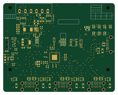
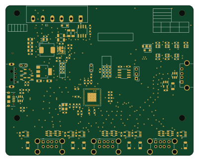
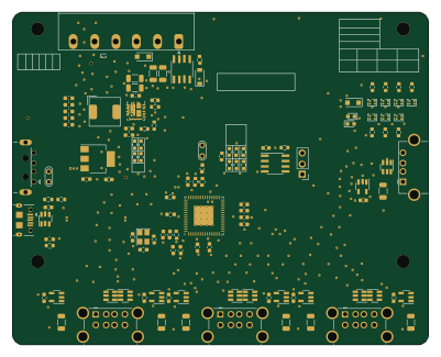
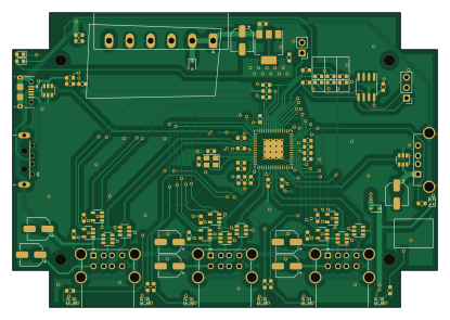
Usb test harness is an open source PCB design by karlp, published on GitHub. It is a 4-layer board measuring 103.6 × 71.8 mm, with 94 components from 44 distinct parts.
Other key parts include the FT24C02A, SE5120ST33, C626667, C211404 and C85364. By type, the board carries 35 capacitors, 21 resistors, 17 ICs, 11 diodes, 8 connectors and 1 crystal.
From the project
Cascading, per port power switching usb2.0-HS 7 port hub
Hubbish is a USB 2.0 HS hub. And? It has per port power switching and overrcurrent shutoff. And? It is designed for cascading, with 6 ports for user devices on the front, and ports on each side for directly plugging together. And? That's it.
Per port power switching was a goal. Also, "this should be really simple!" Also, to make the physical layout sensible for the desired use case. Initially, this project was conceived to be part of regression testing the USB stack for libopencm3. The minimal test setup there required 17 USB devices. This is also why the ports are paired. It's setup to have…
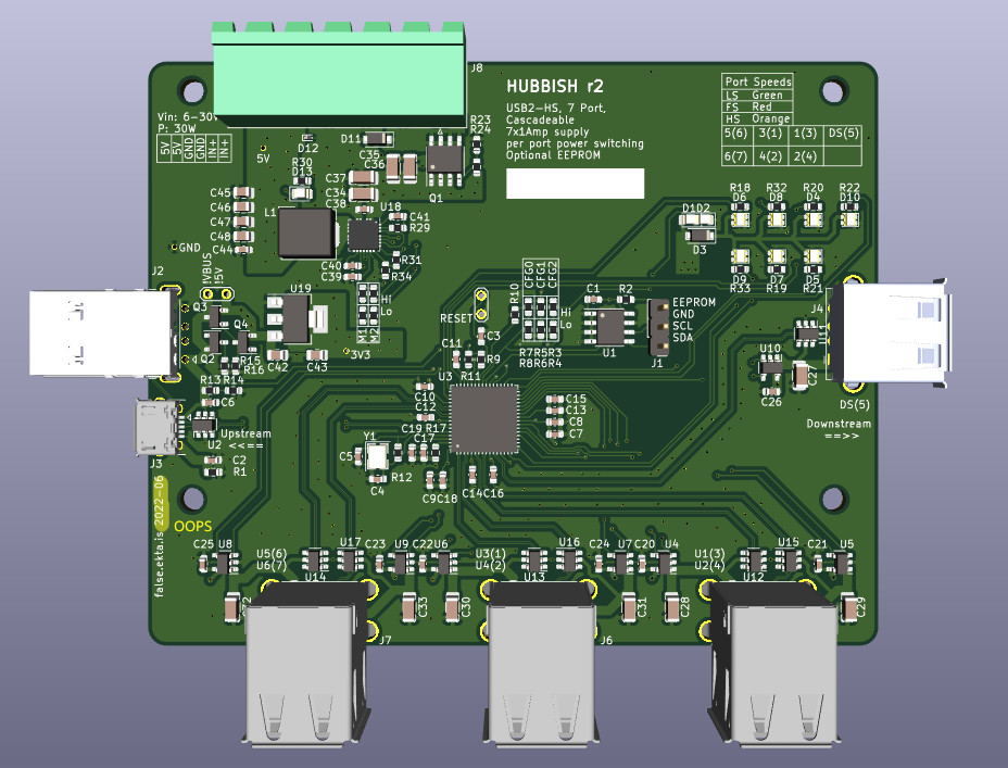
Main components on the Usb test harness
Usb test harness bill of materials (BOM)
94 components, 44 distinct parts — part numbers from the project's BOM.
| Qty | Part | Footprint | Refs |
|---|---|---|---|
| 1 | FT24C02A 2k i2c eeprom | SOIC-8_3.9x4.9mm_P1.27mm | U1 |
| 1 | SE5120ST33 | SOT-223-3_TabPin2 | U2 |
| 1 | C626667 USB2517 | QFN-64-1EP_9x9mm_P0.5mm_EP4.7x4.7mm_ThermalVias | U3 |
| 6 | C211404 APL3511C | SOT-23-5 | U4, U5, U6, U7, U8, U9 |
| 1 | C211404 NUP4202 | SOT-23-6 | U10 |
| 7 | C85364 NUP4202 | SOT-23-6 | U11, U12, U13, U14, U15, U16, U17 |
| 1 | C70590 24MHz | Crystal_SMD_3225-4Pin_3.2x2.5mm | Y1 |
| 1 | Conn_01x06 | PhoenixContact_MSTBA_2,5_6-G-5,08_1x06_P5.08mm_Horizontal | J1 |
| 1 | C42643 or SS-52100 compatible USB_A (female down) | USB_A_Stewart_SS-52100-001_Horizontal | J4 |
| 1 | Conn_01x03_Male | PinHeader_1x03_P2.54mm_Vertical | J5 |
| 3 | USB_A_DUAL | USB_A_Wuerth_61400826021_Horizontal_Stacked | J6, J7, J10 |
| 1 | SOFNG USB-05 USB_A male UP | USB_A_Plug_SOFNG_USB-05 | J8 |
| 1 | U254-051T-4BH23-S2B USB_B_Micro (up) | USB_Micro-B_Amphenol_10118194-0001LF_Horizontal | J9 |
| 1 | Jumper_NO_Small | PinHeader_1x02_P2.54mm_Vertical | JP1 |
| 1 | C84256 SD05-7 | D_SOD-323 | D1 |
| 1 | HS1A | LED_0603_1608Metric | D2 |
| 1 | C64898 HS1B | LED_0603_1608Metric | D3 |
| 6 | C125104 LTST-C295KGKRKT | LED_LiteOn_LTST-C295K | D4, D5, D6, D7, D8, D10 |
| 1 | C125104 D_Small | D_SOD-323 | D9 |
| 1 | LTST-C295KGKRKT | LED_LiteOn_LTST-C295K | D11 |
Show 24 more
| Qty | Part | Footprint | Refs |
|---|---|---|---|
| 2 | C14663 100uF | CP_Elec_5x5.4 | C1, C19 |
| 6 | C14663 .1uF | C_0603_1608Metric | C2, C10, C11, C14, C15, C18 |
| 1 | C14663 2.2uF | C_0603_1608Metric | C3 |
| 2 | C1663 33pF | C_0603_1608Metric | C4, C5 |
| 7 | C15849 1uF | C_0603_1608Metric | C6, C20, C21, C22, C23, C24, C25 |
| 4 | C15849 .1uF | C_0603_1608Metric | C7, C9, C13, C17 |
| 3 | C14663 1uF | C_0603_1608Metric | C8, C12, C16 |
| 1 | C15849 100uF | CP_Elec_5x5.4 | C26 |
| 5 | C15008 100uF | CP_Elec_5x5.4 | C27, C28, C29, C30, C31 |
| 1 | C15008 .1uF | C_0603_1608Metric | C32 |
| 1 | C15008 10uF | C_0603_1608Metric | C33 |
| 1 | C13585 10uF | C_0603_1608Metric | C34 |
| 1 | C13585 .1uF | C_0603_1608Metric | C35 |
| 1 | C23138 10k | R_0603_1608Metric | R1 |
| 4 | C25804 10k | R_0603_1608Metric | R2, R4, R5, R7 |
| 3 | 10k | R_0603_1608Metric | R3, R6, R8 |
| 1 | C25803 100k | R_0603_1608Metric | R9 |
| 5 | C23138 330 | R_0603_1608Metric | R10, R18, R19, R20, R21 |
| 1 | C25804 100k | R_0603_1608Metric | R11 |
| 1 | C22935 100k | R_0603_1608Metric | R12 |
| 1 | C25803 12k | R_0603_1608Metric | R13 |
| 1 | C25803 330 | R_0603_1608Metric | R14 |
| 2 | C25804 330 | R_0603_1608Metric | R15, R16 |
| 1 | C22790 330 | R_0603_1608Metric | R17 |
Usb test harness design files
The KiCad project lives in the karlp/hubbish repository on GitHub; these links point at the commit this page was built from.
Usb test harness: common questions
How big is the Usb test harness PCB?
The Usb test harness measures 103.6 × 71.8 mm, has 4 copper layers and is 1.6 mm thick.
How many components are on the Usb test harness?
94 components, from 44 distinct parts, with part numbers taken from the project's own BOM. The full bill of materials is listed on this page.
Where can I download the Usb test harness design files?
From the karlp/hubbish repository on GitHub, which has the KiCad layout, the schematic and the BOM; the links under Design files point to each one.
Can I use the Usb test harness design in my own project?
The repository has no license, so all rights stay with karlp. Use it as a reference, and ask the author before reusing the design.