TTLINK

About the TTLINK PCB
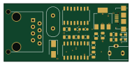
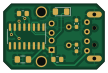
TTLINK is an open source PCB design by kedder, published on GitHub. It is a 2-layer board measuring 26.7 × 17.3 mm, with 10 components from 8 distinct parts.
Other key parts include the CH340G. By type, the board carries 5 capacitors, 2 connectors, 1 IC, 1 crystal and 1 diode.
From the project
PCB design for various electronics projects
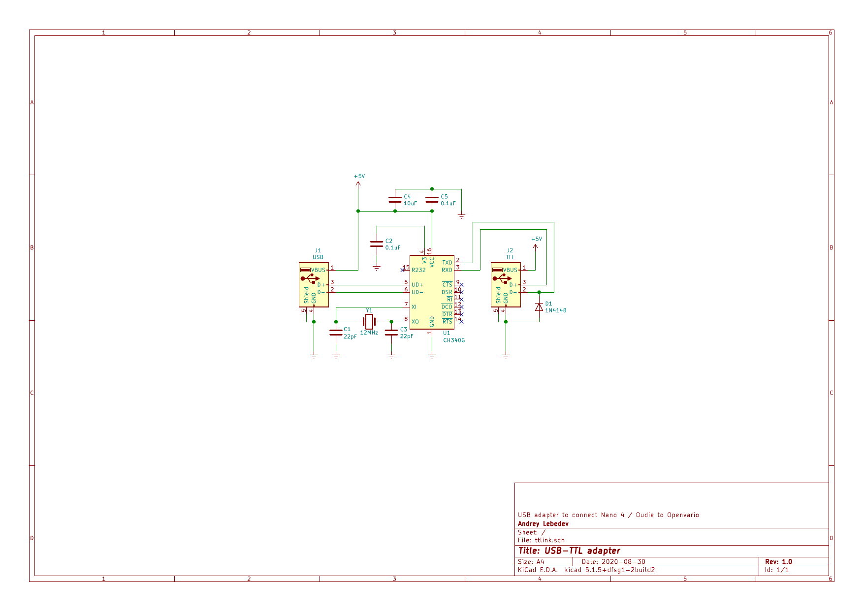
Simple USB adapter to connect devices like LXNAV Nano loggers or Oudie. Even though these devices have a standard micro/mini USB sockets, they do not talk USB protocol with glider electonics. Instead, they use TTL signal. This adapter uses CH340G chip to convert USB protocol to TTL.
Current schematics can be also downloaded in PDF format.
Main components on the TTLINK
TTLINK bill of materials (BOM)
10 components, 8 distinct parts.
| Qty | Part | Footprint | Refs |
|---|---|---|---|
| 1 | CH340G | SOIC-16_3.9x9.9mm_P1.27mm | U1 |
| 1 | 12MHz | Crystal_HC49-4H_Vertical | Y1 |
| 1 | USB | USB2_A_Plug_Horizontal | J1 |
| 1 | TTL | USB_A_Stewart_SS-52100-001_Horizontal | J2 |
| 1 | 1N4148 | D_1206_3216Metric_Pad1.42x1.75mm_HandSolder | D1 |
| 2 | 22pF | C_0603_1608Metric_Pad1.05x0.95mm_HandSolder | C1, C3 |
| 2 | 0.1uF | C_0805_2012Metric_Pad1.15x1.40mm_HandSolder | C2, C5 |
| 1 | 10uF | C_1206_3216Metric_Pad1.42x1.75mm_HandSolder | C4 |
TTLINK design files
The KiCad project lives in the kedder/kedhw repository on GitHub; these links point at the commit this page was built from.
- Layoutttlink/ttlink.kicad_pcb
TTLINK: common questions
How big is the TTLINK PCB?
The TTLINK measures 26.7 × 17.3 mm, has 2 copper layers and is 1.6 mm thick.
How many components are on the TTLINK?
10 components, from 8 distinct parts. The full bill of materials is listed on this page.
Where can I download the TTLINK design files?
From the kedder/kedhw repository on GitHub, which has the KiCad layout; the links under Design files point to each one.
Can I use the TTLINK design in my own project?
The repository has no license, so all rights stay with kedder. Use it as a reference, and ask the author before reusing the design.