
Wireless proj

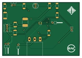
About the Wireless proj PCB
Wireless proj is an open source PCB design by lzyang2000, published on GitHub. It is a 2-layer board measuring 77.9 × 54.6 mm, with 19 components from 16 distinct parts.
Other key parts include the LT6106 and LM7805CT_Obsolete. By type, the board carries 4 connectors, 4 resistors, 2 ICs, 2 diodes, 2 capacitors and 1 module.
It belongs with the iot & wireless designs in this gallery.
Main components on the Wireless proj
Wireless proj bill of materials (BOM)
19 components, 16 distinct parts — part numbers from the project's BOM.
| Qty | Part | Footprint | Refs |
|---|---|---|---|
| 1 | LT6106 | SOT-23-8 | U1 |
| 1 | LM7805CT_Obsolete | FanPinHeader_1x03_P2.54mm_Vertical | U2 |
| 1 | Q_NMOS_DGS | TO-3P-3_Horizontal_TabDown | M1 |
| 1 | Conn_01x02_Male | PinHeader_1x02_P2.54mm_Horizontal | J1 |
| 2 | Conn_01x01_Male | PinHeader_1x01_P2.54mm_Horizontal | J2, J3 |
| 1 | Conn_01x02_Female | PinHeader_1x02_P2.54mm_Vertical | J4 |
| 1 | Conn_01x02_Male | PinHeader_1x02_P2.54mm_Horizontal | P_in1 |
| 1 | 200 | R_2010_5025Metric_Pad1.52x2.65mm_HandSolder | Rl1 |
| 1 | Thermistor | R_2010_5025Metric_Pad1.52x2.65mm_HandSolder | TH1 |
| 1 | LED | LED_D5.0mm | LED1 |
| 1 | D_Schottky_ALT | D_2512_6332Metric_Pad1.52x3.35mm_HandSolder | D1 |
| 1 | D_Schottky | D_3220_8050Metric_Pad2.65x5.15mm_HandSolder | D2 |
| 2 | 10u | C_1812_4532Metric_Pad1.30x3.40mm_HandSolder | C1, C2 |
| 1 | 1 | R_2010_5025Metric_Pad1.52x2.65mm_HandSolder | R1 |
| 2 | 200 | R_2010_5025Metric_Pad1.52x2.65mm_HandSolder | R2, R3 |
| 1 | 4.99k | R_2010_5025Metric_Pad1.52x2.65mm_HandSolder | R4 |
Wireless proj design files
The KiCad project lives in the lzyang2000/PCB-Projects repository on GitHub; these links point at the commit this page was built from.
Wireless proj: common questions
How big is the Wireless proj PCB?
The Wireless proj measures 77.9 × 54.6 mm, has 2 copper layers and is 1.6 mm thick.
How many components are on the Wireless proj?
19 components, from 16 distinct parts, with part numbers taken from the project's own BOM. The full bill of materials is listed on this page.
Where can I download the Wireless proj design files?
From the lzyang2000/PCB-Projects repository on GitHub, which has the KiCad layout and the BOM; the links under Design files point to each one.
Can I use the Wireless proj design in my own project?
The repository has no license, so all rights stay with lzyang2000. Use it as a reference, and ask the author before reusing the design.
More boards in PCB-Projects
Similar boards
EinkPDA screen
TalismanDesign
95 × 54 mm27 parts2LApache-2.02.0k
RPi RM0 WiFi/Bluetooth Module
schlae
11.1 × 14 mm76 parts6LNo license1.0k
L0 USB
Luos-io
20.3 × 15.3 mm19 parts2LMIT547
Breakout board
26.7 × 27.9 mm29 parts2LMIT547
Stm32f0 disco Luos shield
55.9 × 99.1 mm26 parts2LMIT547
L0 USBA
20.3 × 15.3 mm19 parts2LMIT547