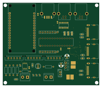
PCB panel

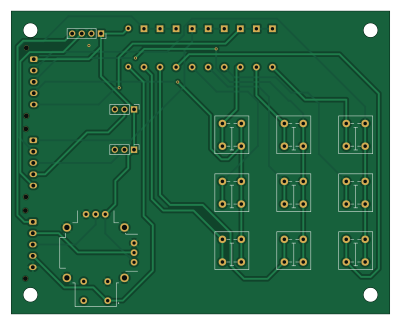
About the PCB panel
PCB panel is an open source PCB design by Mattkomi, published on GitHub. It is a 2-layer board measuring 100 × 80 mm, with 26 components from 10 distinct parts.
Other key parts include the Joystick and OLed screen. By type, the board carries 11 switches, 9 diodes, 3 connectors, 2 ICs and 1 resistor.
From the project
PFE 2024-2025 Polytech SIR, projet Visio
Simplifier la gestion des équipements grâce à une interface centralisée. Automatiser des tâches fréquentes, comme l'affichage des participants sur l'écran de retour ou le lancement d'applications utilisées régulièrement. Reproduire, tout en innovant, les fonctionnalités de l'interface StarLeaf. Ce projet a été réalisé dans le cadre du PFE VISIO de la filière Polytech SIR par :
Main components on the PCB panel
PCB panel bill of materials (BOM)
26 components, 10 distinct parts.
| Qty | Part | Footprint | Refs |
|---|---|---|---|
| 1 | Joystick | XDCR_COM-09032 | U1 |
| 1 | OLed screen | PinSocket_1x04_P2.54mm_Vertical | U2 |
| 1 | Conn 1 | Molex_Micro-Fit_3.0_43650-0515_1x05_P3.00mm_Vertical | J1 |
| 1 | Conn 2 | Molex_Micro-Fit_3.0_43650-0515_1x05_P3.00mm_Vertical | J2 |
| 1 | Conn 3 | Molex_Micro-Fit_3.0_43650-0515_1x05_P3.00mm_Vertical | J3 |
| 9 | SW_Push | PVA1 OA H1 1.2N V2 | SW1, SW2, SW3, SW4, SW5, SW6, SW7, SW8 +1 |
| 1 | SW_USB | PinHeader_1x03_P2.54mm_Vertical | SW10 |
| 1 | SW_HDMI | PinHeader_1x03_P2.54mm_Vertical | SW11 |
| 9 | D | D_A-405_P10.16mm_Horizontal | D1, D2, D3, D4, D5, D6, D7, D8 +1 |
| 1 | 10K | R_Axial_DIN0207_L6.3mm_D2.5mm_P10.16mm_Horizontal | R1 |
PCB panel design files
The KiCad project lives in the Mattkomi/Poly_Leaf repository on GitHub; these links point at the commit this page was built from.
- LayoutPCB_panel/PCB_panel.kicad_pcb
- SchematicPCB_panel/PCB_panel.kicad_sch
PCB panel: common questions
How big is the PCB panel?
The PCB panel measures 100 × 80 mm, has 2 copper layers and is 1.6 mm thick.
How many components are on the PCB panel?
26 components, from 10 distinct parts. The full bill of materials is listed on this page.
Where can I download the PCB panel design files?
From the Mattkomi/Poly_Leaf repository on GitHub, which has the KiCad layout and the schematic; the links under Design files point to each one.
Can I use the PCB panel design in my own project?
The repository has no license, so all rights stay with Mattkomi. Use it as a reference, and ask the author before reusing the design.