
Logic analyzer adapter

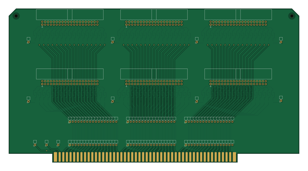
About the Logic analyzer adapter PCB
Logic analyzer adapter is an open source PCB design by mnarigon, published on GitHub under the MIT license. It is a 2-layer board measuring 254 × 134.6 mm, with 332 components from 18 distinct parts.
By type, the board carries 204 resistors, 102 capacitors and 24 connectors.
It belongs with the test & measurement designs in this gallery.
From the project
An S-100 bus logic analyzer adapter board
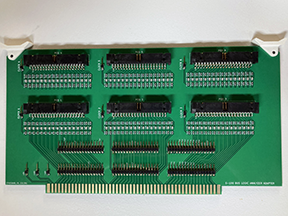
This is an S-100 bus logic analyzer adapter board. It simplifies the connection to the S-100 bus of common 40-pin pod cables like those for older HP/Agilent/Keysight logic analyzers.
See the Keysight document, Probing Solutions for Logic Analyzers, for more information on the pod interface.
Note that the photo is of the prototype board.
The design files are revision A, and have some changes based on my experience with the prototype board. I haven't had the revision A boards manufactured since the prototype is working for my purposes.
Logic analyzer adapter bill of materials (BOM)
332 components, 18 distinct parts — part numbers from the project's BOM.
| Qty | Part | Footprint | Refs |
|---|---|---|---|
| 6 | MHE40E CONN_02x20 3M 2540-5002 | IDC_Header_02x20_P2.54mm_RA | J1, J2, J3, J8, J9, J10 |
| 1 | ORDERONEADDITIONAL2057-PH1RB-17-UA CLOCK_4 | PinHeader_01x01_P2.54mm_RA | J4 |
| 1 | ORDERONEADDITIONAL2057-PH1RB-17-UA CLOCK_5 | PinHeader_01x01_P2.54mm_RA | J5 |
| 1 | ORDERONEADDITIONAL2057-PH1RB-17-UA CLOCK_6 | PinHeader_01x01_P2.54mm_RA | J6 |
| 1 | ORDERONEADDITIONAL2057-PH1RB-17-UA EXTRA_2 | PinHeader_01x01_P2.54mm_RA | J7 |
| 1 | ORDERONEADDITIONAL2057-PH1RB-17-UA EXTRA_1 | PinHeader_01x01_P2.54mm_RA | J11 |
| 1 | ORDERONEADDITIONAL2057-PH1RB-17-UA CLOCK_1 | PinHeader_01x01_P2.54mm_RA | J12 |
| 1 | ORDERONEADDITIONAL2057-PH1RB-17-UA CLOCK_2 | PinHeader_01x01_P2.54mm_RA | J13 |
| 1 | ORDERONEADDITIONAL2057-PH1RB-17-UA CLOCK_3 | PinHeader_01x01_P2.54mm_RA | J14 |
| 6 | 2057-PH1RB-17-UA CONN_01x17 | PinHeader_01x17_P2.54mm_RA | J15, J16, J17, J21, J22, J23 |
| 1 | ORDERONEADDITIONAL2057-PH1RB-17-UA +8_V | PinHeader_01x01_P2.54mm_RA | J18 |
| 1 | ORDERONEADDITIONAL2057-PH1RB-17-UA +16_V | PinHeader_01x01_P2.54mm_RA | J19 |
| 1 | ORDERONEADDITIONAL2057-PH1RB-17-UA -16_V | PinHeader_01x01_P2.54mm_RA | J20 |
| 1 | S100_MALE | S100_MALE | P1 |
| 2 | CardEjector | CardEjector | H1, H2 |
| 102 | 8.2PF 8.2pF | C_0805 | C1, C2, C3, C4, C5, C6, C7, C8 +94 |
| 102 | RMCF0805FT90K9 90.9K | R_0805 | R1, R2, R3, R4, R5, R6, R7, R8 +94 |
| 102 | RMCF0805FT249R 249 | R_0805 | R52, R53, R54, R55, R56, R57, R58, R59 +94 |
Logic analyzer adapter design files
The KiCad project lives in the mnarigon/logic-analyzer-adapter repository on GitHub; these links point at the commit this page was built from.
Logic analyzer adapter: common questions
How big is the Logic analyzer adapter PCB?
The Logic analyzer adapter measures 254 × 134.6 mm, has 2 copper layers and is 1.6 mm thick.
How many components are on the Logic analyzer adapter?
332 components, from 18 distinct parts, with part numbers taken from the project's own BOM. The full bill of materials is listed on this page.
Where can I download the Logic analyzer adapter design files?
From the mnarigon/logic-analyzer-adapter repository on GitHub, which has the KiCad layout, the schematic and the BOM; the links under Design files point to each one.
Can I use the Logic analyzer adapter design in my own project?
Yes, under the terms of its MIT license, which mnarigon chose for the repository.
Similar boards
AnalyzerBoxPCB fork
gusmanb
52.7 × 47.9 mm54 parts4LGPL-3.05.0k
LevelShifter
28.3 × 39.8 mm21 parts2LGPL-3.05.0k
StackLink
52.3 × 10.5 mm5 parts2LGPL-3.05.0k
EleLab v2 Frontpanel a
Chrismettal
88 × 25 mm23 parts2LGPL-3.0528
EleLab v2 Bus150
150 × 50 mm37 parts2LGPL-3.0528
EleLab v2 PowerFeed
68 × 50 mm11 parts2LGPL-3.0528