Nucleo

About the Nucleo PCB
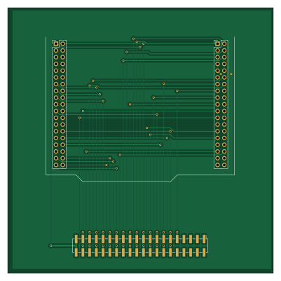
Nucleo is an open source PCB design by nailed-barnacle, published on GitHub under the MIT license. It is a 2-layer board measuring 100 × 100 mm, with 3 components from 2 distinct parts.
From the project
A cut-down version of the 8080 processor using HCTTL and including a discrete ALU and instruction decoder
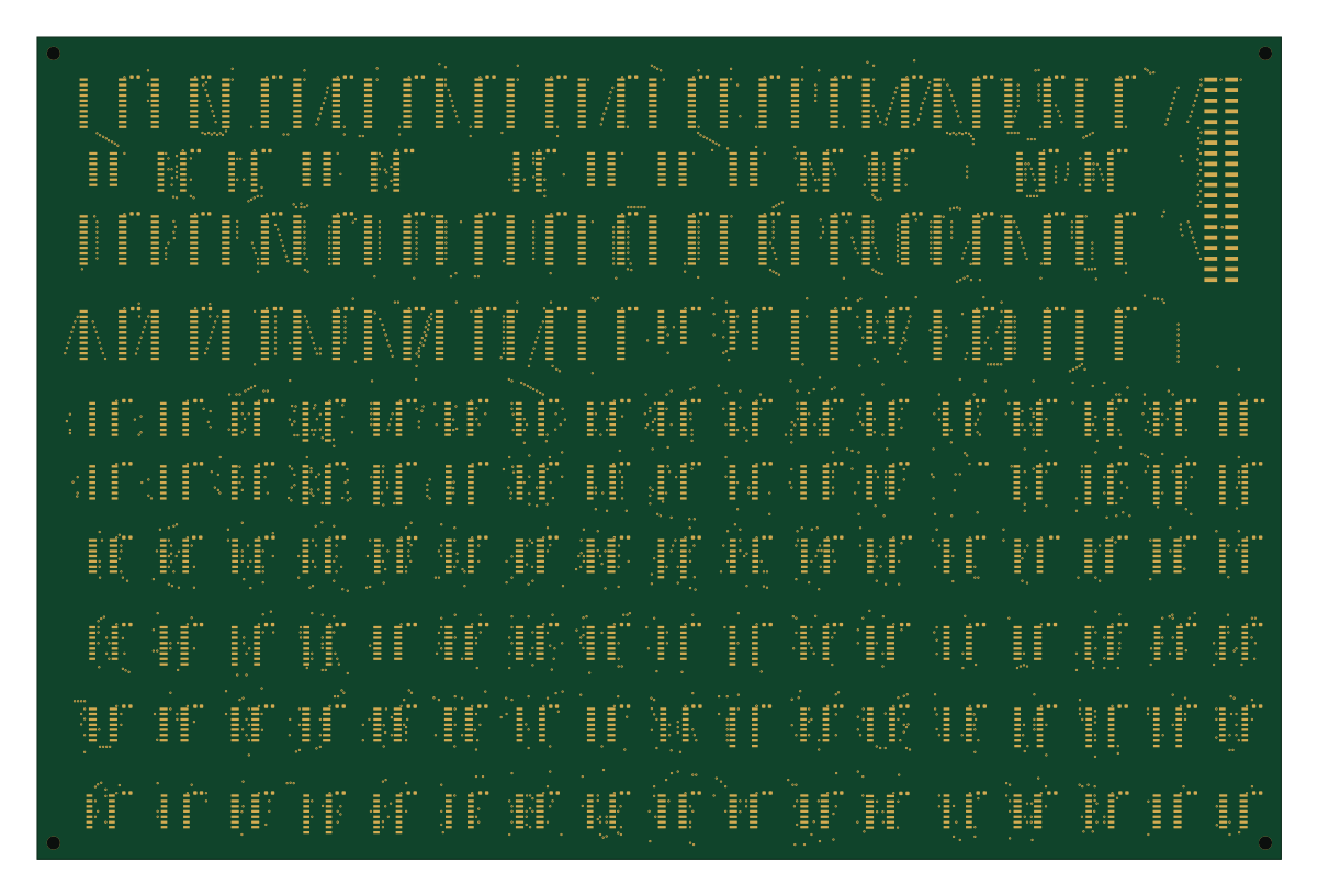
This is an attempt to replicate most of the functionality of the 1970s Intel 8080 processor using contemporary HCTTL surface mount components.
By implementing most - though by no means all - of the instructions of the 8080 it allows the use of existing toolchains to generate code for the device both for the hardware implementation and the associated simulation.
Nucleo bill of materials (BOM)
3 components, 2 distinct parts — part numbers from the project's BOM.
| Qty | Part | Footprint | Refs |
|---|---|---|---|
| 1 | Conn_02x20_Odd_Even | PinHeader_2x20_P2.54mm_Vertical_SMD | J1 |
| 2 | Conn_02x19_Odd_Even | PinHeader_2x19_P2.54mm_Vertical | J2, J3 |
Nucleo design files
The KiCad project lives in the nailed-barnacle/Cisc-8-ttl-processor repository on GitHub; these links point at the commit this page was built from.
Nucleo: common questions
How big is the Nucleo PCB?
The Nucleo measures 100 × 100 mm, has 2 copper layers and is 1.6 mm thick.
How many components are on the Nucleo?
3 components, from 2 distinct parts, with part numbers taken from the project's own BOM. The full bill of materials is listed on this page.
Where can I download the Nucleo design files?
From the nailed-barnacle/Cisc-8-ttl-processor repository on GitHub, which has the KiCad layout and the BOM; the links under Design files point to each one.
Can I use the Nucleo design in my own project?
Yes, under the terms of its MIT license, which nailed-barnacle chose for the repository.