
Usb c solder tester vcut

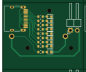
About the Usb c solder tester vcut PCB
Usb c solder tester vcut is an open source PCB design by Netetra, published on GitHub. It is a 2-layer board measuring 30 × 25 mm, with 21 components from 5 distinct parts.
By type, the board carries 9 diodes, 9 resistors, 2 connectors and 1 battery holder.
Usb c solder tester vcut bill of materials (BOM)
21 components, 5 distinct parts — part numbers from the project's BOM.
| Qty | Part | Footprint | Refs |
|---|---|---|---|
| 1 | USB_C_RECEPTACLE_USB2.0_16P USB_C_Receptacle_USB2.0_16P | USB_C_Receptacle_HRO_TYPE-C-31-M-12 | J1 |
| 1 | CONN_01X02_PIN Conn_01x02_Pin | PinHeader_1x02_P2.54mm_Horizontal | J2 |
| 1 | Battery_Cell | CH25-2032LF | BT1 |
| 9 | LED | LED_0603_1608Metric | D1, D2, D3, D4, D5, D6, D7, D8 +1 |
| 9 | 1kΩ | R_0603_1608Metric | R1, R2, R3, R4, R5, R6, R7, R8 +1 |
Usb c solder tester vcut design files
The KiCad project lives in the Netetra/kicad-archive repository on GitHub; these links point at the commit this page was built from.
Usb c solder tester vcut: common questions
How big is the Usb c solder tester vcut PCB?
The Usb c solder tester vcut measures 30 × 25 mm, has 2 copper layers and is 1.6 mm thick.
How many components are on the Usb c solder tester vcut?
21 components, from 5 distinct parts, with part numbers taken from the project's own BOM. The full bill of materials is listed on this page.
Where can I download the Usb c solder tester vcut design files?
From the Netetra/kicad-archive repository on GitHub, which has the KiCad layout and the BOM; the links under Design files point to each one.
Can I use the Usb c solder tester vcut design in my own project?
The repository has no license, so all rights stay with Netetra. Use it as a reference, and ask the author before reusing the design.
More boards in kicad-archive
 STM32
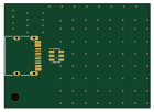
STM32F303k8-led matrix-4layer
35 × 25 mm98 parts4LNo license0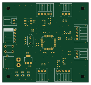 STM32
STM32New-3ch motor control
75 × 70 mm62 parts2LNo license0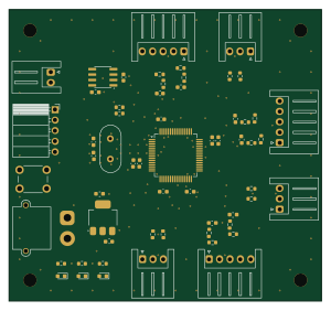 STM32
STM323ch motor control
75 × 70 mm62 parts2LNo license0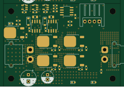
Dc v1 vcut
61 × 43 mm46 parts2LNo license0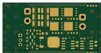
Dc for-385-v2 vcut
50 × 25 mm44 parts2LNo license0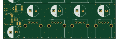
Ch334-usbhub vcut
95 × 30 mm34 parts2LNo license0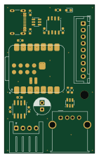 ESP32
ESP32Esp32s3-main v1
34 × 56 mm22 parts4LNo license0 WCH CH32/CH55x
Ch552-daplink vcut
22 × 11.5 mm21 parts2LNo license0
Ch340-usb uart vcut
28.5 × 12.3 mm19 parts2LNo license0
Ne555-servo tester vcut
90 × 90 mm17 parts2LNo license0