NerMo Electronics Stack II

About the NerMo Electronics Stack II PCB
NerMo Electronics Stack II is an open source PCB design by NoMoreBrainToUse, published on GitHub. It is a 2-layer board measuring 50.5 × 21 mm, with 31 components from 22 distinct parts.
Other key parts include the PCA9685PW. By type, the board carries 17 connectors, 11 resistors, 2 capacitors and 1 IC.
From the project
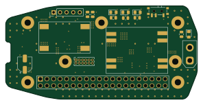
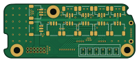
The electronics stack consists of two PCB.
The electronics stack consists of two PCB.
The first main PCB is the main EPS PCB. It contains most of the components including DCDC for 5V, 6V, 3V3, connection to Raspberry Zero 2W, power switch and power indication LED, as well as onboard power monitoring for all three voltage bus via the INA3221, onboard MPU6050 with external connection option, as well as connector to the PWM Driver PCB.
Main components on the NerMo Electronics Stack II
NerMo Electronics Stack II bill of materials (BOM)
31 components, 22 distinct parts — part numbers from the project's BOM.
| Qty | Part | Footprint | Refs |
|---|---|---|---|
| 1 | PCA9685PW | TSSOP-28_4.4x9.7mm_P0.65mm | U5 |
| 1 | PWM 5 | JST_SH_SM03B-SRSS-TB_1x03-1MP_P1.00mm_Horizontal | J1 |
| 1 | CONN_02X06_ODD_EVEN Conn_02x06_Odd_Even | PinHeader_2x06_P1.27mm_Vertical | J2 |
| 1 | PWM 1 | JST_SH_SM03B-SRSS-TB_1x03-1MP_P1.00mm_Horizontal | J3 |
| 1 | PWM 2 | JST_SH_SM03B-SRSS-TB_1x03-1MP_P1.00mm_Horizontal | J5 |
| 1 | PWM 3 | JST_SH_SM03B-SRSS-TB_1x03-1MP_P1.00mm_Horizontal | J6 |
| 1 | PWM 4 | JST_SH_SM03B-SRSS-TB_1x03-1MP_P1.00mm_Horizontal | J7 |
| 1 | PWM 6 | JST_SH_SM03B-SRSS-TB_1x03-1MP_P1.00mm_Horizontal | J8 |
| 1 | PWM 7 | JST_SH_SM03B-SRSS-TB_1x03-1MP_P1.00mm_Horizontal | J9 |
| 1 | PWM 8 | JST_SH_SM03B-SRSS-TB_1x03-1MP_P1.00mm_Horizontal | J10 |
| 1 | PWM 9 | JST_SH_SM03B-SRSS-TB_1x03-1MP_P1.00mm_Horizontal | J11 |
| 1 | PWM 10 | JST_SH_SM03B-SRSS-TB_1x03-1MP_P1.00mm_Horizontal | J12 |
| 1 | PWM 11 | JST_SH_SM03B-SRSS-TB_1x03-1MP_P1.00mm_Horizontal | J13 |
| 1 | PWM 12 | JST_SH_SM03B-SRSS-TB_1x03-1MP_P1.00mm_Horizontal | J14 |
| 1 | PWM 13 | JST_SH_BM03B-SRSS-TB_1x03-1MP_P1.00mm_Vertical | J15 |
| 1 | PWM 14 | JST_SH_BM03B-SRSS-TB_1x03-1MP_P1.00mm_Vertical | J16 |
| 1 | PWM 15 | JST_SH_BM03B-SRSS-TB_1x03-1MP_P1.00mm_Vertical | J17 |
| 1 | PWM 16 | JST_SH_BM03B-SRSS-TB_1x03-1MP_P1.00mm_Vertical | J18 |
| 1 | 470 µF | CP_EIA-7360-38_Kemet-E_HandSolder | C1 |
| 1 | 10UF 10uF | C_0603_1608Metric | C4 |
Show 2 more
| Qty | Part | Footprint | Refs |
|---|---|---|---|
| 7 | 10K 10k | R_0603_1608Metric | R12, R13, R14, R15, R16, R17, R18 |
| 4 | 220 | R_Array_Concave_4x0603 | RN1, RN2, RN3, RN4 |
NerMo Electronics Stack II design files
The KiCad project lives in the NoMoreBrainToUse/electrical-NerMo-Electronic-Stack repository on GitHub; these links point at the commit this page was built from.
NerMo Electronics Stack II: common questions
How big is the NerMo Electronics Stack II PCB?
The NerMo Electronics Stack II measures 50.5 × 21 mm, has 2 copper layers and is 1.6 mm thick.
How many components are on the NerMo Electronics Stack II?
31 components, from 22 distinct parts, with part numbers taken from the project's own BOM. The full bill of materials is listed on this page.
Where can I download the NerMo Electronics Stack II design files?
From the NoMoreBrainToUse/electrical-NerMo-Electronic-Stack repository on GitHub, which has the KiCad layout, the schematic and the BOM; the links under Design files point to each one.
Can I use the NerMo Electronics Stack II design in my own project?
The repository has no license, so all rights stay with NoMoreBrainToUse. Use it as a reference, and ask the author before reusing the design.