
Stamp-Board of-AD8232

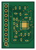
About the Stamp-Board of-AD8232
Stamp-Board of-AD8232 is an open source PCB design by nwasr, published on GitHub under the MIT license. It is a 2-layer board measuring 17.5 × 24.7 mm, with 23 components from 13 distinct parts.
Other key parts include the AD8232ACPZ-R7. By type, the board carries 14 resistors, 7 capacitors, 1 IC and 1 connector.
From the project
Compact AD8232 stamp board designed in KiCad v9 with schematic, PCB layout, Gerbers, BOM, and 3D view.
This repository contains the KiCad v9 design files for a compact AD8232 stamp board, built according to Figure 66 of the AD8232 datasheet.
- Compact Form Factor – Optimized layout for minimal space usage - Standardized Terminals – VDD, GND, LO+, LO-, OUT, nSDN, LA, RA, RL - Proper Grounding – Copper pours on top and bottom layers for improved signal integrity - Manufacturing-Ready – Includes Gerber files, BOM, and 3D visualization
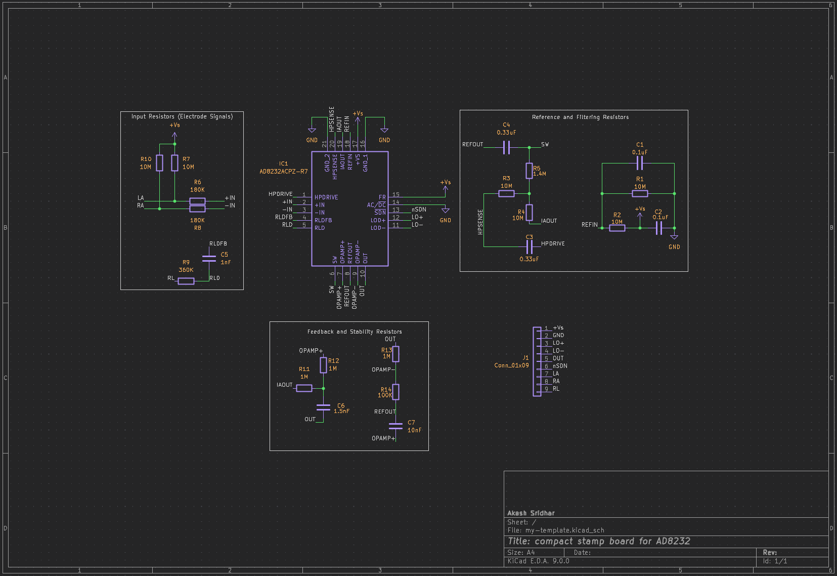
Main components on the Stamp-Board of-AD8232
Stamp-Board of-AD8232 bill of materials (BOM)
23 components, 13 distinct parts — part numbers from the project's BOM.
| Qty | Part | Footprint | Refs |
|---|---|---|---|
| 1 | AD8232ACPZ-R7 | CP_20_10_ADI | IC1 |
| 1 | CONN_01X09 Conn_01x09 | PinHeader_1x09_P2.54mm_Vertical | J1 |
| 2 | 0.1UF 0.1uF | C_0402_1005Metric | C1, C2 |
| 2 | 0.33UF 0.33uF | C_0402_1005Metric | C3, C4 |
| 1 | 1NF 1nF | C_0402_1005Metric | C5 |
| 1 | 1.5NF 1.5nF | C_0402_1005Metric | C6 |
| 1 | 10NF 10nF | C_0402_1005Metric | C7 |
| 6 | 10M | R_0402_1005Metric | R1, R2, R3, R4, R7, R10 |
| 1 | 1.4M | R_0402_1005Metric | R5 |
| 2 | 180K | R_0402_1005Metric | R6, R8 |
| 1 | 360K | R_0402_1005Metric | R9 |
| 3 | 1M | R_0402_1005Metric | R11, R12, R13 |
| 1 | 100K | R_0402_1005Metric | R14 |
Stamp-Board of-AD8232 design files
The KiCad project lives in the nwasr/Stamp-Board-of-AD8232 repository on GitHub; these links point at the commit this page was built from.
Stamp-Board of-AD8232: common questions
How big is the Stamp-Board of-AD8232?
The Stamp-Board of-AD8232 measures 17.5 × 24.7 mm, has 2 copper layers and is 1.6 mm thick.
How many components are on the Stamp-Board of-AD8232?
23 components, from 13 distinct parts, with part numbers taken from the project's own BOM. The full bill of materials is listed on this page.
Where can I download the Stamp-Board of-AD8232 design files?
From the nwasr/Stamp-Board-of-AD8232 repository on GitHub, which has the KiCad layout, the schematic and the BOM; the links under Design files point to each one.
Can I use the Stamp-Board of-AD8232 design in my own project?
Yes, under the terms of its MIT license, which nwasr chose for the repository.