
Daughterboard

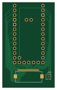
About the Daughterboard PCB
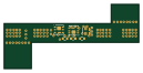
Daughterboard is an open source PCB design by Ovens-Syntax, published on GitHub under the GPL-3.0 license. It is a 2-layer board measuring 27.9 × 45.4 mm, with 3 components from 3 distinct parts.
It belongs with the keyboards and dev boards & breakouts designs in this gallery.
From the project
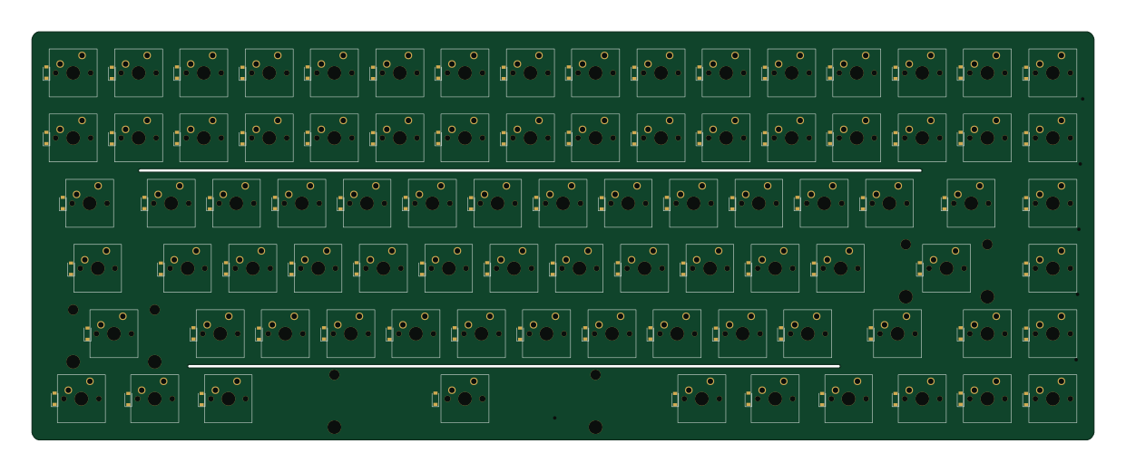
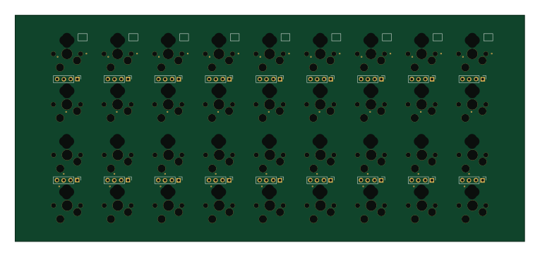
a keyboard pcb by me with a slightly tweaked 75% layout (sorry im too lazy to integrate mcu so matrix pcb connects to dauter/dev board)
Daughterboard bill of materials (BOM)
3 components, 3 distinct parts — part numbers from the project's BOM.
| Qty | Part | Footprint | Refs |
|---|---|---|---|
| 1 | TSW-102-23-T-S Conn_01x22_Male Samtec | Hirose_FH12-22S-0.5SH_1x22-1MP_P0.50mm_Horizontal | J2 |
| 1 | TSW-118-23-T-D Conn_01x03_Male Samtec | PinSocket_1x03_P1.27mm_Vertical | J3 |
| 1 | TSW-118-23-T-D helios Samtec | helios | J4 |
Daughterboard design files
The KiCad project lives in the Ovens-Syntax/Steam75 repository on GitHub; these links point at the commit this page was built from.
Daughterboard: common questions
How big is the Daughterboard PCB?
The Daughterboard measures 27.9 × 45.4 mm, has 2 copper layers and is 1.6 mm thick.
How many components are on the Daughterboard?
3 components, from 3 distinct parts, with part numbers taken from the project's own BOM. The full bill of materials is listed on this page.
Where can I download the Daughterboard design files?
From the Ovens-Syntax/Steam75 repository on GitHub, which has the KiCad layout, the schematic and the BOM; the links under Design files point to each one.
Can I use the Daughterboard design in my own project?
Yes, under the terms of its GPL-3.0 license, which Ovens-Syntax chose for the repository.
 byrantech


 google