
EDA-

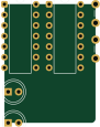
About the EDA- PCB
EDA- is an open source PCB design by Pengyang-uestc, published on GitHub. It is a 2-layer board measuring 22 × 28.5 mm, with 6 components from 4 distinct parts.
Other key parts include the SW, XOR, AND and LED.
From the project
“工业软件创新训练 I”四人课程项目,使用 C++17、wxWidgets 3.2 和 CMake。
“工业软件创新训练 I”四人课程项目,使用 C++17、wxWidgets 3.2 和 CMake。
在画布上放置逻辑门、连接引脚,点击开关验证 0/1 逻辑,保存工程或导出文件到 KiCad。
先安装 Visual Studio 2022 的“使用 C++ 的桌面开发”(含 CMake 工具),准备 wxWidgets 3.2 的 x64 静态库。首次配置见新人上手指南。
更新入口要求工作区干净且当前分支有远程跟踪分支;有本地修改、拉取失败、编译失败或测试失败时停止。它不会自动提交、暂存或覆盖改动。Git 只更新源码,程序仍需编译;入口会自动完成增量编译。
打开示例:程序中选择“文件 → 打开”,选择 docs/样例/半加器/halfadder.eda`,按 F5 后点击开关。
- 6 种逻辑门、开关、指示灯,共 8 种内置元件;支持用真值表定义双输入、单输出元件。 - 放置、移动、连线、框选、复制粘贴、删除、撤销和重做。 - 0/1 组合逻辑仿真,导线按逻辑值着色,指示灯显示输出。 - .eda 工程存档;KiCad 网表导入/导出;KiCad 原理图导出。
Main components on the EDA-
EDA- bill of materials (BOM)
6 components, 4 distinct parts.
| Qty | Part | Footprint | Refs |
|---|---|---|---|
| 2 | SW | SW_PUSH_6mm | U1, U2 |
| 1 | XOR | DIP-14_W7.62mm | U3 |
| 1 | AND | DIP-14_W7.62mm | U4 |
| 2 | LED | LED_D5.0mm | U5, U6 |
EDA- design files
The KiCad project lives in the Pengyang-uestc/EDA- repository on GitHub; these links point at the commit this page was built from.
EDA-: common questions
How big is the EDA- PCB?
The EDA- measures 22 × 28.5 mm, has 2 copper layers and is 1.6 mm thick.
How many components are on the EDA-?
6 components, from 4 distinct parts. The full bill of materials is listed on this page.
Where can I download the EDA- design files?
From the Pengyang-uestc/EDA- repository on GitHub, which has the KiCad layout and the schematic; the links under Design files point to each one.
Can I use the EDA- design in my own project?
The repository has no license, so all rights stay with Pengyang-uestc. Use it as a reference, and ask the author before reusing the design.