
HighVoltageBoard

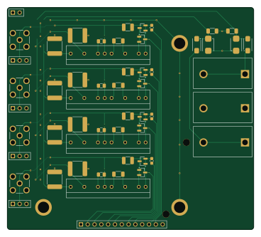
About the HighVoltageBoard PCB
HighVoltageBoard is an open source PCB design by philipturner, published on GitHub under the MIT license. It is a 2-layer board measuring 91.9 × 82.5 mm, with 53 components from 16 distinct parts.
Other key parts include the PA95. By type, the board carries 14 resistors, 12 capacitors, 8 transistors, 8 connectors, 4 ICs and 4 diodes.
From the project
Objective: Finish a project that has dragged on for 14 months.
Objective: Finish a project that has dragged on for 14 months.
Deadline: April 31, 2026 for creepless imaging of graphite
$80,000 worth of wire transfers have hit the bank. I now have enough financial security to proceed with hardware work.
The first step is ensuring I can be paid a full-time salary. Comply with US tax laws, SEC regulations, etc. I predicted the exact numbers before going through the legal boilerplate and setup.
Main components on the HighVoltageBoard
HighVoltageBoard bill of materials (BOM)
53 components, 16 distinct parts.
| Qty | Part | Footprint | Refs |
|---|---|---|---|
| 4 | PA95 | PA95 | U1, U2, U3, U4 |
| 8 | Q_NJFET_DSG | SOT-23 | Q1, Q2, Q3, Q4, Q5, Q6, Q7, Q8 |
| 1 | Conn_01x13_Socket | PinSocket_1x13 | J1 |
| 1 | Banana Socket, Green | Multicomp_24.243 | J3 |
| 1 | Banana Socket, Black | Multicomp_24.243 | J4 |
| 1 | Banana Socket, Blue | Multicomp_24.243 | J5 |
| 4 | Conn_Coaxial | RFPC-SMA27-F | J6, J9, J12, J15 |
| 3 | Mounting Hole, M2.5 | Keystone_24929 | H1, H2, H4 |
| 2 | Vr = 2 kV | DO-214AC | D1, D2 |
| 2 | Vr = 451V | DO-214AA | D3, D4 |
| 8 | 47 nF, 630V | CAPC2220_GRJ | C1, C2, C4, C5, C7, C8, C10, C11 |
| 4 | 10 pF, 1 kV | CAPC1206_CHV | C3, C6, C9, C12 |
| 2 | 1M, 5%, 0.33W, 800V | RESC1206_RCV | R1, R2 |
| 4 | 28k, 0.1% | RESC0603 | R3, R6, R9, R12 |
| 4 | 1M, 0.1%, 0.33W, 1 kV | RESC1210_TNPV | R4, R7, R10, R13 |
| 4 | 15, 1%, 0.25W, 1.9V | RESC0805 | R5, R8, R11, R14 |
HighVoltageBoard design files
The KiCad project lives in the philipturner/capacitive-displacement-metrology repository on GitHub; these links point at the commit this page was built from.
HighVoltageBoard: common questions
How big is the HighVoltageBoard PCB?
The HighVoltageBoard measures 91.9 × 82.5 mm, has 2 copper layers and is 1.6256 mm thick.
How many components are on the HighVoltageBoard?
53 components, from 16 distinct parts. The full bill of materials is listed on this page.
Where can I download the HighVoltageBoard design files?
From the philipturner/capacitive-displacement-metrology repository on GitHub, which has the KiCad layout and the schematic; the links under Design files point to each one.
Can I use the HighVoltageBoard design in my own project?
Yes, under the terms of its MIT license, which philipturner chose for the repository.
More boards in capacitive-displacement-metrology
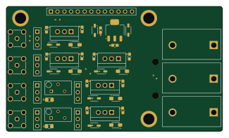
PowerBoard
81.1 × 47.1 mm18 parts2LMIT5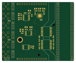
MainBoard
77 × 62.5 mm12 parts4LMIT5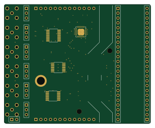
MainBoard1
77 × 62.5 mm10 parts4LMIT5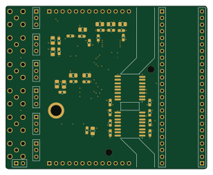
MainBoard2
77 × 62.5 mm9 parts4LMIT5
PreAmp
23 × 11.4 mm8 parts2LMIT5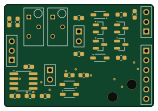
TIA2 Post
39.3 × 26.9 mm5 parts2LMIT5
TIA2 Pre
21.8 × 19 mm4 parts2LMIT5
TIA1
21.8 × 19 mm4 parts2LMIT5