
TIA1


About the TIA1 PCB
TIA1 is an open source PCB design by philipturner, published on GitHub under the MIT license. It is a 2-layer board measuring 21.8 × 19 mm, with 4 components from 3 distinct parts.
Other key parts include the OPA828. By type, the board carries 2 connectors, 1 IC and 1 resistor.
From the project
Objective: Finish a project that has dragged on for 14 months.
Objective: Finish a project that has dragged on for 14 months.
Deadline: April 31, 2026 for creepless imaging of graphite
$80,000 worth of wire transfers have hit the bank. I now have enough financial security to proceed with hardware work.
The first step is ensuring I can be paid a full-time salary. Comply with US tax laws, SEC regulations, etc. I predicted the exact numbers before going through the legal boilerplate and setup.
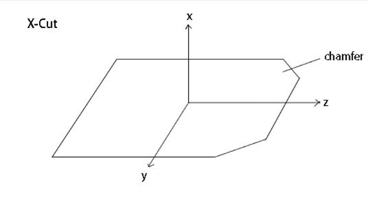
Main components on the TIA1
TIA1 bill of materials (BOM)
4 components, 3 distinct parts.
| Qty | Part | Footprint | Refs |
|---|---|---|---|
| 1 | OPA828 | SOIC-8 | U1 |
| 2 | Conn_01x08_Socket | PinSocket_1x8 | J2, J3 |
| 1 | 100M, 5%, 0603 | RESC0603 | R1 |
TIA1 design files
The KiCad project lives in the philipturner/capacitive-displacement-metrology repository on GitHub; these links point at the commit this page was built from.
- LayoutModels/TIA1/TIA1.kicad_pcb
- SchematicModels/TIA1/TIA1.kicad_sch
TIA1: common questions
How big is the TIA1 PCB?
The TIA1 measures 21.8 × 19 mm, has 2 copper layers and is 1.6256 mm thick.
How many components are on the TIA1?
4 components, from 3 distinct parts. The full bill of materials is listed on this page.
Where can I download the TIA1 design files?
From the philipturner/capacitive-displacement-metrology repository on GitHub, which has the KiCad layout and the schematic; the links under Design files point to each one.
Can I use the TIA1 design in my own project?
Yes, under the terms of its MIT license, which philipturner chose for the repository.
More boards in capacitive-displacement-metrology
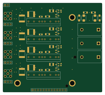
HighVoltageBoard
91.9 × 82.5 mm53 parts2LMIT5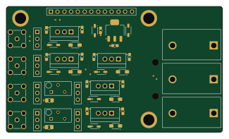
PowerBoard
81.1 × 47.1 mm18 parts2LMIT5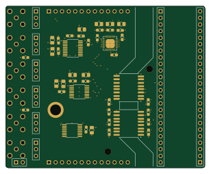
MainBoard
77 × 62.5 mm12 parts4LMIT5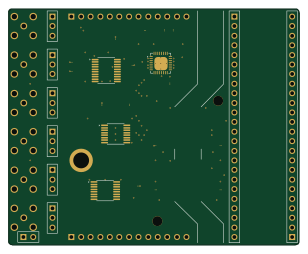
MainBoard1
77 × 62.5 mm10 parts4LMIT5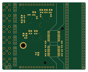
MainBoard2
77 × 62.5 mm9 parts4LMIT5
PreAmp
23 × 11.4 mm8 parts2LMIT5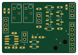
TIA2 Post
39.3 × 26.9 mm5 parts2LMIT5
TIA2 Pre
21.8 × 19 mm4 parts2LMIT5