
Mems breakout

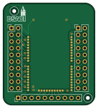
About the Mems breakout
Mems breakout is an open source PCB design by PisterLab, published on GitHub. It is a 2-layer board measuring 34.9 × 38.7 mm, with 8 components from 3 distinct parts.
It belongs with the dev boards & breakouts designs in this gallery.
From the project
PCBs to break out MEMS bond pads for testing
This repo contains KiCad projects for PCBs designed to break out MEMS devices for research/development.
This PCB is contained in the memsbreakoutw50/ directory and provides 50 connections from wire bond pads on the MEMS die that are routed to standard pitch (2.54mm) headers.
Gerbers & drill files are provided for manufacturing at memsbreakoutw50/memsbreakoutw5-v0gerbersdrillfiles.zip
Mems breakout bill of materials (BOM)
8 components, 3 distinct parts.
| Qty | Part | Footprint | Refs |
|---|---|---|---|
| 2 | Conn_02x10_Counter_Clockwise | PinHeader_2x10_P2.54mm_Vertical | J1, J8 |
| 5 | Conn_01x10_Male | wirebondarray-dteal | J2, J3, J5, J6, J7 |
| 1 | Conn_01x10_Male | PinHeader_1x10_P2.54mm_Vertical | J4 |
Mems breakout design files
The KiCad project lives in the PisterLab/mems-breakout-pcb repository on GitHub; these links point at the commit this page was built from.
Mems breakout: common questions
How big is the Mems breakout?
The Mems breakout measures 34.9 × 38.7 mm, has 2 copper layers and is 1.6 mm thick.
How many components are on the Mems breakout?
8 components, from 3 distinct parts. The full bill of materials is listed on this page.
Where can I download the Mems breakout design files?
From the PisterLab/mems-breakout-pcb repository on GitHub, which has the KiCad layout and the schematic; the links under Design files point to each one.
Can I use the Mems breakout design in my own project?
The repository has no license, so all rights stay with PisterLab. Use it as a reference, and ask the author before reusing the design.
Similar boards
134pin 7-967288-1
rusefi
139.7 × 73.7 mm38 parts2LGPL-3.01.2k
Breakout 112pin Connector
174 × 58 mm39 parts2LGPL-3.01.2k
Breakout 60pin EEC-IV
139.7 × 62.2 mm15 parts2LGPL-3.01.2k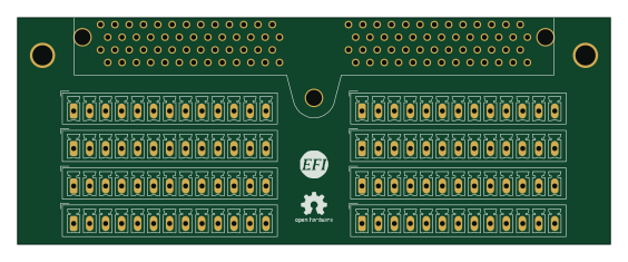
Eecv breakout
140.8 × 53.7 mm9 parts4LGPL-3.01.2k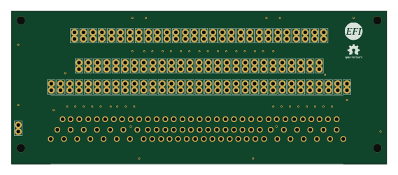
88 Pin Vag Breakout
142 × 58 mm91 parts2LGPL-3.01.2k
Rj45 breakout
rene-dev
15.2 × 53.8 mm3 parts2LGPL-3.0979