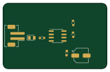
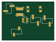
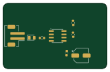
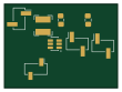
Snap Adapter 17up 150x100

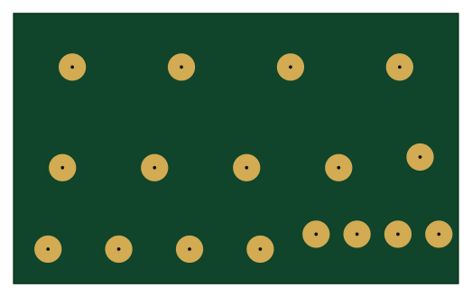
About the Snap Adapter 17up 150x100 PCB
Snap Adapter 17up 150x100 is an open source PCB design by Pluze, published on GitHub under the MIT license. It is a 2-layer board measuring 130.5 × 79.3 mm, with 17 components from 5 distinct parts.
From the project
Reference and experimental KiCad PCB designs with reusable agent workflows
This design family adapts circular thin-film electrodes to an exposed front copper pad intended for soldering a snap connector. Each board has one centered contact on each side and one centered drilled hole. The front contact is fixed at 8 mm; the back contact follows the thin-film electrode diameter.
The boards are intended for in-house fabrication on an LPKF U4. The machine does not create a plated barrel in this workflow, so the center hole is a manual interconnect: wick solder through the 1.0 mm drill to join the front and back copper, then verify continuity before attaching the film…

Snap Adapter 17up 150x100 bill of materials (BOM)
17 components, 5 distinct parts — part numbers from the project's BOM.
| Qty | Part | Footprint | Refs |
|---|---|---|---|
| 3 | FRONT_8mm_BACK_20mm | Circular_Contact_Asymmetric | J1, J2, J4 |
| 1 | SNT-100-BK-T FRONT_8mm_BACK_20mm Samtec | Circular_Contact_Asymmetric | J3 |
| 4 | FRONT_8mm_BACK_15mm | Circular_Contact_Asymmetric | J5, J6, J7, J8 |
| 5 | FRONT_8mm_BACK_10mm | Circular_Contact_Asymmetric | J9, J10, J11, J12, J13 |
| 4 | FRONT_8mm_BACK_5mm | Circular_Contact_Asymmetric | J14, J15, J16, J17 |
Snap Adapter 17up 150x100 design files
The KiCad project lives in the Pluze/pcb repository on GitHub; these links point at the commit this page was built from.
Snap Adapter 17up 150x100: common questions
How big is the Snap Adapter 17up 150x100 PCB?
The Snap Adapter 17up 150x100 measures 130.5 × 79.3 mm, has 2 copper layers and is 1.6 mm thick.
How many components are on the Snap Adapter 17up 150x100?
17 components, from 5 distinct parts, with part numbers taken from the project's own BOM. The full bill of materials is listed on this page.
Where can I download the Snap Adapter 17up 150x100 design files?
From the Pluze/pcb repository on GitHub, which has the KiCad layout and the BOM; the links under Design files point to each one.
Can I use the Snap Adapter 17up 150x100 design in my own project?
Yes, under the terms of its MIT license, which Pluze chose for the repository.