Split

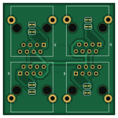
About the Split PCB
Split is an open source PCB design by ppetr, published on GitHub under the Apache-2.0 license. It is a 2-layer board measuring 42 × 42 mm, with 4 components from 1 distinct parts.
From the project
SW and HW for an inexpensive home automation communication network based on the CAN bus
Disclaimer: This is not an officially supported Google product._
This project aims to create both SW and HW for an inexpensive home automation communication network based on the CAN bus using common components and infrastructure.
Eventually it will contain hardware plans (KiCAD) and software to control individual modules.
At the moment subdirectories contain work in progress, untested, and not suitable for any use whatsoever.
Split bill of materials (BOM)
4 components, 1 distinct parts.
| Qty | Part | Footprint | Refs |
|---|---|---|---|
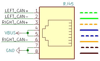
| 4 | RJ45_Shielded | RJ45_Ninigi_GE | J1, J2, J3, J4 |
Split design files
The KiCad project lives in the ppetr/home-automation-CAN repository on GitHub; these links point at the commit this page was built from.
- Layoutsplit/split.kicad_pcb
Split: common questions
How big is the Split PCB?
The Split measures 42 × 42 mm, has 2 copper layers and is 1.6 mm thick.
How many components are on the Split?
4 components, from 1 distinct parts. The full bill of materials is listed on this page.
Where can I download the Split design files?
From the ppetr/home-automation-CAN repository on GitHub, which has the KiCad layout; the links under Design files point to each one.
Can I use the Split design in my own project?
Yes, under the terms of its Apache-2.0 license, which ppetr chose for the repository.