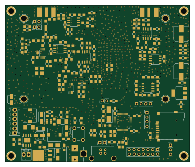
Daughterboard

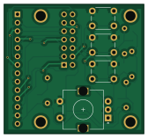
About the Daughterboard PCB
Daughterboard is an open source PCB design by profdc9, published on GitHub. It is a 2-layer board measuring 42 × 39 mm, with 18 components from 14 distinct parts.
By type, the board carries 8 resistors, 5 connectors and 4 switches.
From the project
Vector Network Analyzer based on the STM32F103C8T6 bluepill
This a project to create a Vector Network Analyzer based on the EU1KY antenna tuner that can be reconfigured for different needs. This material is copyrighted by Daniel Marks (KW4TI) and licensed under the Creative Commons License CC-BY-SA 4.0. The software is licensed under the zlib license. These are open source licenses that permit commercial use, modification and redistribution with attribution, and require licensees to assume all risk for using the copyrighted materials.
Daughterboard bill of materials (BOM)
18 components, 14 distinct parts — part numbers from the project's BOM.
| Qty | Part | Footprint | Refs |
|---|---|---|---|
| 1 | CONN_02X07_ODD_EVEN Conn_02x07_Odd_Even | Pin_Header_Straight_2x07_Pitch2.54mm | J1 |
| 3 | Conn_01x01 | 1pin | J2, J4, J5 |
| 1 | CONN_01X04 Conn_01x01 | 1pin | J3 |
| 1 | ILIdisplay | Pin_Header_Straight_1x14_Pitch2.54mm | DISP1 |
| 1 | SW_DPDT_X2 SW_Push | SW_PUSH_6mm | SW1 |
| 1 | SW_DIP_X01 Rotary_Encoder_Switch_Alps | RotaryEncoder_Alps_EC11E-Switch_Vertical_H20mm | SW2 |
| 2 | SW_Push | SW_PUSH_6mm | SW3, SW4 |
| 2 | 10K 100k | R_0805_HandSoldering | R1, R7 |
| 1 | 10K 100k | R_Axial_DIN0207_L6.3mm_D2.5mm_P7.62mm_Horizontal | R2 |
| 1 | 100k | R_0805_HandSoldering | R3 |
| 1 | 680R 100k | R_Axial_DIN0207_L6.3mm_D2.5mm_P7.62mm_Horizontal | R4 |
| 1 | 47R 100k | R_0805_HandSoldering | R5 |
| 1 | 4R7 100k | R_Axial_DIN0207_L6.3mm_D2.5mm_P7.62mm_Horizontal | R6 |
| 1 | 1K5 100k | R_Axial_DIN0207_L6.3mm_D2.5mm_P7.62mm_Horizontal | R8 |
Daughterboard design files
The KiCad project lives in the profdc9/VNA repository on GitHub; these links point at the commit this page was built from.
Daughterboard: common questions
How big is the Daughterboard PCB?
The Daughterboard measures 42 × 39 mm, has 2 copper layers and is 1.6 mm thick.
How many components are on the Daughterboard?
18 components, from 14 distinct parts, with part numbers taken from the project's own BOM. The full bill of materials is listed on this page.
Where can I download the Daughterboard design files?
From the profdc9/VNA repository on GitHub, which has the KiCad layout and the BOM; the links under Design files point to each one.
Can I use the Daughterboard design in my own project?
The repository has no license, so all rights stay with profdc9. Use it as a reference, and ask the author before reusing the design.