
VNA

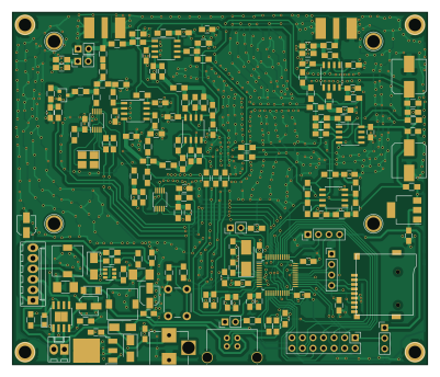
About the VNA PCB
VNA is an open source STM32 PCB design by profdc9, published on GitHub. It is a 2-layer board measuring 100 × 85 mm, with 178 components from 63 distinct parts.
Its main chip is the STM32F103C8T6, from the STM32 family. Other key parts include the SI5351A, LM393, SA612, LM358 and AMS1117-3V3. By type, the board carries 64 resistors, 60 capacitors, 16 connectors, 14 ICs, 9 inductors and 5 jumpers.
From the project
Vector Network Analyzer based on the STM32F103C8T6 bluepill
This a project to create a Vector Network Analyzer based on the EU1KY antenna tuner that can be reconfigured for different needs. This material is copyrighted by Daniel Marks (KW4TI) and licensed under the Creative Commons License CC-BY-SA 4.0. The software is licensed under the zlib license. These are open source licenses that permit commercial use, modification and redistribution with attribution, and require licensees to assume all risk for using the copyrighted materials.
Main components on the VNA
VNA bill of materials (BOM)
178 components, 63 distinct parts — part numbers from the project's BOM.
| Qty | Part | Footprint | Refs |
|---|---|---|---|
| 2 | SI5351A | MSOP-10_3x3mm_Pitch0.5mm | U1, U12 |
| 1 | LM393 | SOIC-8_3.9x4.9mm_Pitch1.27mm | U2 |
| 3 | SA612 | SOIC-8_3.9x4.9mm_Pitch1.27mm | U3, U4, U5 |
| 2 | LM358 | SOIC-8_3.9x4.9mm_Pitch1.27mm | U6, U7 |
| 1 | AMS1117-3V3 | SOT-223 | U8 |
| 1 | 78M05_TO252 | TO-252-3_TabPin2 | U9 |
| 1 | MT3608 | SOT-23-6 | U10 |
| 1 | CN3052 | TI_SO-PowerPAD-8 | U11 |
| 1 | MicroSD_SPI_CD | GCT-MEM2055-00-190-01-A | U13 |
| 1 | STM32F103C8T6 | LQFP-48_7x7mm_Pitch0.5mm | U14 |
| 1 | 2SC3356 | SOT-23 | Q3 |
| 1 | C9006 25 MHz | Crystal_SMD_3225-4pin_3.2x2.5mm_HandSoldering | Y1 |
| 1 | C115962 8 MHz | Crystal_SMD_5032-2pin_5.0x3.2mm_HandSoldering | Y2 |
| 1 | CONN_02X07_ODD_EVEN Conn_02x07_Odd_Even | Pin_Header_Straight_2x07_Pitch2.54mm | J1 |
| 2 | Conn_Coaxial | Amphenol_RF_SMA_132289 | J2, J9 |
| 2 | CONN_01X04 Conn_01x04 | Pin_Header_Straight_1x04_Pitch2.54mm | J3, J10 |
| 8 | CONN_01X01 Conn_01x01 | 1pin | J8, J11, J14, J16, J18, J19, J20, J21 |
| 1 | Barrel_Jack | BARREL_JACK | J13 |
| 1 | CONN_01X02 Conn_01x02 | Molex_KK-6410-02_02x2.54mm_Straight | J15 |
| 1 | USB_B | USB_B | J24 |
Show 43 more
| Qty | Part | Footprint | Refs |
|---|---|---|---|
| 4 | Jumper_NC_Small | Pin_Header_Straight_1x02_Pitch2.54mm | JP1, JP2, JP3, JP7 |
| 1 | Jumper_NC_Dual | Pin_Header_Straight_1x03_Pitch2.54mm | JP5 |
| 1 | SW_DPDT_X2 SW_DPDT_x2 | Molex_KK-6410-06_06x2.54mm_Straight | SW1 |
| 1 | SW_DIP_X01 SW_DIP_x01 | SW_PUSH_6mm | SW2 |
| 3 | SS14 | D_SMA | D3, D4, D5 |
| 1 | MMSZ5232B | D_MiniMELF | D6 |
| 1 | LED | LED_0805 | D7 |
| 7 | C1015 Ferrite_Bead_Small | L_0805_HandSoldering | L1, L2, L3, L4, L5, L6, L7 |
| 2 | 10 uH | L_7.3x7.3_H4.5 | L9, L10 |
| 38 | 100 nF | C_0805_HandSoldering | C1, C2, C3, C5, C6, C8, C9, C10 +30 |
| 2 | 1000 uF | CP_Elec_8x10.5 | C4, C7 |
| 3 | 330 pF | C_0805_HandSoldering | C14, C15, C16 |
| 3 | 10 nF | C_0805_HandSoldering | C26, C27, C28 |
| 3 | 68 pF | C_0805_HandSoldering | C29, C30, C31 |
| 3 | 1 nF | C_0805_HandSoldering | C34, C35, C36 |
| 2 | 22 uF | C_1210_HandSoldering | C38, C44 |
| 1 | 4.7 uF | CP_Elec_4x4.5 | C45 |
| 1 | 1 uF | C_0805_HandSoldering | C47 |
| 1 | 10 uF | CP_Elec_4x4.5 | C49 |
| 1 | 100 uF | CP_Elec_4x4.5 | C52 |
| 2 | 22 pF | C_0805_HandSoldering | C58, C60 |
| 13 | 10K 10k | R_0805_HandSoldering | R1, R2, R7, R10, R36, R37, R38, R39 +5 |
| 5 | 1k | R_0805_HandSoldering | R3, R28, R29, R32, R42 |
| 1 | 680R | R_0805_HandSoldering | R4 |
| 1 | 47R 51R | R_0805_HandSoldering | R5 |
| 2 | 4R7 1R | R_0805_HandSoldering | R6, R13 |
| 12 | 1K5 1k5 | R_0805_HandSoldering | R8, R9, R19, R20, R21, R25, R26, R27 +4 |
| 1 | 47R 82R | R_0805_HandSoldering | R11 |
| 4 | 51R | R_0805_HandSoldering | R14, R16, R44, R46 |
| 1 | 220R 51R | R_0805_HandSoldering | R15 |
| 1 | 4R7 | R_0805_HandSoldering | R17 |
| 1 | 47R | R_0805_HandSoldering | R18 |
| 3 | 100K 100k | R_0805_HandSoldering | R22, R23, R24 |
| 3 | 2K2 2k2 | R_0805_HandSoldering | R30, R31, R33 |
| 2 | 1M | R_0805_HandSoldering | R34, R35 |
| 3 | C17477 0R | R_0805_HandSoldering | R41, R50, R63 |
| 2 | 22R | R_0805_HandSoldering | R47, R48 |
| 2 | 220R | R_0805_HandSoldering | R51, R58 |
| 1 | 270R | R_0805_HandSoldering | R57 |
| 3 | 100R | R_0805_HandSoldering | R59, R61, R62 |
| 1 | 68R | R_0805_HandSoldering | R60 |
| 1 | 120R | R_0805_HandSoldering | R67 |
| 1 | 22R 1R | R_0805_HandSoldering | R68 |
VNA design files
The KiCad project lives in the profdc9/VNA repository on GitHub; these links point at the commit this page was built from.
VNA: common questions
What microcontroller does the VNA use?
The VNA is built around the STM32F103C8T6, from the STM32 family.
How big is the VNA PCB?
The VNA measures 100 × 85 mm, has 2 copper layers and is 1.6 mm thick.
How many components are on the VNA?
178 components, from 63 distinct parts, with part numbers taken from the project's own BOM. The full bill of materials is listed on this page.
Where can I download the VNA design files?
From the profdc9/VNA repository on GitHub, which has the KiCad layout and the BOM; the links under Design files point to each one.
Can I use the VNA design in my own project?
The repository has no license, so all rights stay with profdc9. Use it as a reference, and ask the author before reusing the design.
Can I test firmware for the VNA without the hardware?
Yes. HardLabs builds a simulation of the board from its netlist and BOM, so you can run and debug STM32 firmware against it before you order a PCB.
More boards in VNA
Similar boards
 STM32
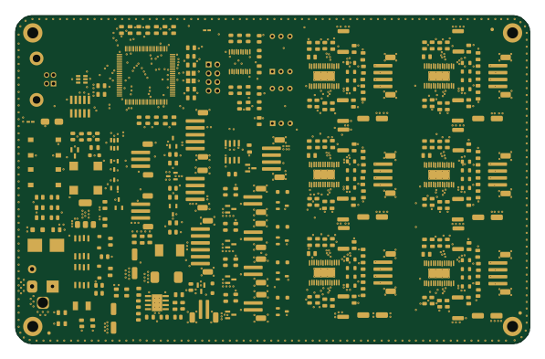
LumenPnP Motherboard
opulo-inc
149 × 95 mm296 parts4LCC-BY-SA-4.03.7k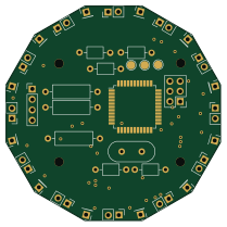 STM32
Base
google
52.3 × 52.3 mm36 parts2LApache-2.02.9k STM32
Type g
169 × 30 mm24 parts2LApache-2.02.9k STM32
Main panel
234 × 84 mm26 parts4LApache-2.02.9k STM32
Type a
150 × 30 mm14 parts2LApache-2.02.9k STM32
Type c
188 × 30 mm17 parts2LApache-2.02.9k