
Ps2usb

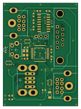
About the Ps2usb PCB
Ps2usb is an open source WCH CH32/CH55x PCB design by rasteri, published on GitHub. It is a 2-layer board measuring 40 × 55 mm, with 25 components from 13 distinct parts.
Its main chip is the CH559L, from the WCH CH32/CH55x family. Other key parts include the MAX232IDR. By type, the board carries 12 capacitors, 4 connectors, 3 resistors, 2 ICs, 1 crystal and 1 fuse.
It belongs with the keyboards designs in this gallery.
From the project
Adapting USB devices to work on old computers
HIDman is an open source device to allow the use of modern USB keyboards and mice on legacy PCs.
Peripherals that support legacy PCs are becoming hard to find, especially for the very first PCs. This project aims to provide a simple cheap solution that will cover everything from the original IBM 5150 PC all the way up to modern computers that have PS/2 ports.
Main components on the Ps2usb
Ps2usb bill of materials (BOM)
25 components, 13 distinct parts — part numbers from the project's BOM.
| Qty | Part | Footprint | Refs |
|---|---|---|---|
| 1 | CH559L CH559L-less WCH | QFP-12x12_14x14_Pitch0.5mm | U1 |
| 1 | MAX232IDR MAX232 Texas Instruments | SOIC-16_3.9x9.9mm_P1.27mm | U2 |
| 1 | X322512MSB4SI 12MHz YXC | Crystal_SMD_3225-4Pin_3.2x2.5mm | Y1 |
| 2 | DIN-603 DIN8 HOOYA | DIN8 | J1, J3 |
| 1 | USB1035 | USB1035 | J2 |
| 1 | Conn_01x03_Pin | PinHeader_1x03_P2.54mm_Vertical | J5 |
| 1 | BSMD1206-050-30V 500mA BHFUSE | Fuse_1206_3216Metric | F1 |
| 1 | KH-6X6X9H-ZJ RATACSWITCH Shenzhen Kinghelm Elec | TS11 | S1 |
| 1 | P4-1204RGBWS2-1.5T-A B3173BGR-20C0001Q3U1930 TUOZHAN | B3173BGR-20C0001Q3U1930 | D1 |
| 10 | CL10A335KP8NNNC 3.3u Samsung | C_0603_1608Metric | C1, C2, C3, C4, C6, C7, C8, C9 +2 |
| 2 | CC0603JRNPO9BN100 10pF YAGEO | C_0603_1608Metric | C5, C11 |
| 2 | YC164-FR-071KL 1K YAGEO | R_Array_Convex_4x0603 | RN1, RN2 |
| 1 | YC164-JR-07120RL 150 YAGEO | R_Array_Convex_4x0603 | RN3 |
Ps2usb design files
The KiCad project lives in the rasteri/HIDman repository on GitHub; these links point at the commit this page was built from.
Ps2usb: common questions
What microcontroller does the Ps2usb use?
The Ps2usb is built around the CH559L, from the WCH CH32/CH55x family.
How big is the Ps2usb PCB?
The Ps2usb measures 40 × 55 mm, has 2 copper layers and is 1.6 mm thick.
How many components are on the Ps2usb?
25 components, from 13 distinct parts, with part numbers taken from the project's own BOM. The full bill of materials is listed on this page.
Where can I download the Ps2usb design files?
From the rasteri/HIDman repository on GitHub, which has the KiCad layout, the schematic and the BOM; the links under Design files point to each one.
Can I use the Ps2usb design in my own project?
The repository has no license, so all rights stay with rasteri. Use it as a reference, and ask the author before reusing the design.
Can I test firmware for the Ps2usb without the hardware?
Yes. HardLabs builds a simulation of the board from its netlist and BOM, so you can run and debug WCH CH32/CH55x firmware against it before you order a PCB.
Similar boards
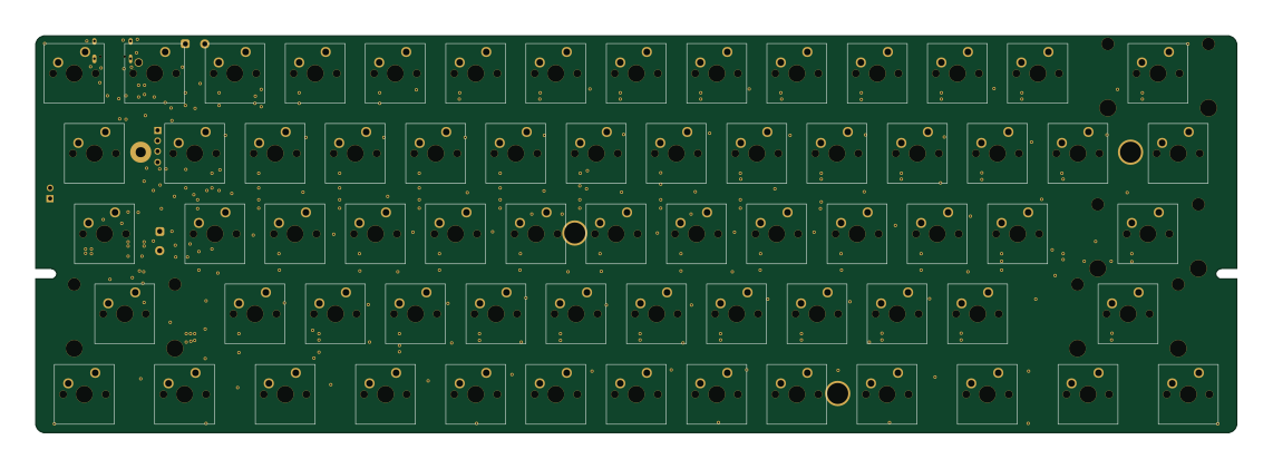 WCH CH32/CH55x
CH32X-60-ANSI-Improved
rgoulter
285 × 94.2 mm149 parts2LNo license230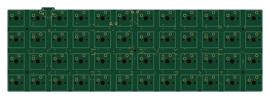 WCH CH32/CH55x
CH552-48
224.6 × 74.2 mm107 parts2LNo license230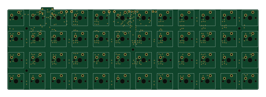 WCH CH32/CH55x
CH32X-48
224.6 × 74.2 mm112 parts2LNo license230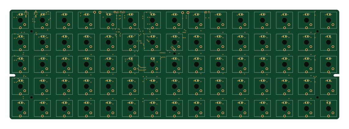 WCH CH32/CH55x
CH32X-75
285 × 94.2 mm318 parts2LNo license230 WCH CH32/CH55x
Webusb programmer rev6
laneboysrc
38 × 20 mm18 parts2LMIT87 WCH CH32/CH55x
Idawgz32
ChrisChrisLoLo
98.7 × 45.5 mm81 parts2LGPL-3.077