
Two site-Automated-Testbed for-Evaluating-ADCs

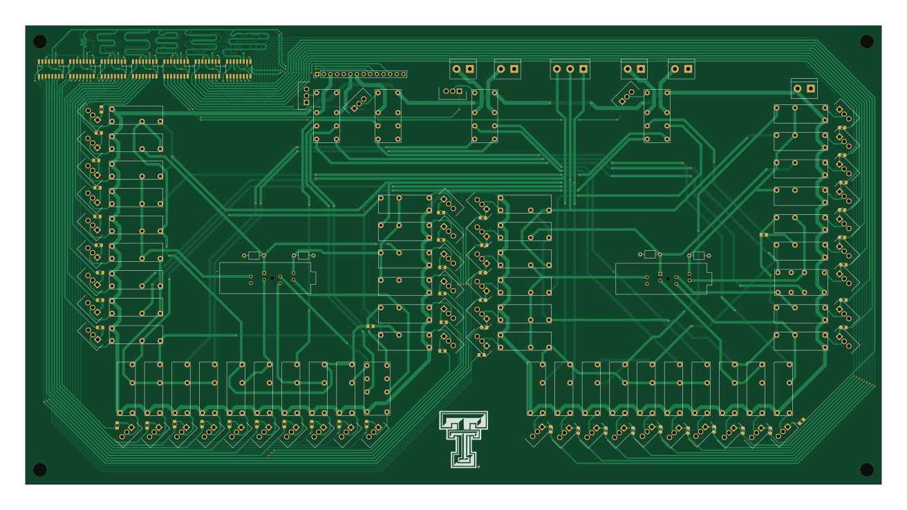
About the Two site-Automated-Testbed for-Evaluating-ADCs PCB
Two site-Automated-Testbed for-Evaluating-ADCs is an open source PCB design by rishikesh2715, published on GitHub under the MIT license. It is a 2-layer board measuring 327.5 × 175.5 mm, with 238 components from 19 distinct parts.
Other key parts include the 74LVC595AD,118. By type, the board carries 109 resistors, 54 relays, 53 transistors, 9 connectors, 7 ICs and 4 capacitors.
It belongs with the test & measurement designs in this gallery.
From the project
The Two-site Automated Test System (ATS-2) is a custom-designed testbed for evaluating ADCs, specifically focused on testing the ADS7816. This comprehensive testing solution consists of a custom-designed device interface board, National Instruments VirtualBench integration, and automated test programs implemented in Python.
- DPDT Relay: J104D2C24VDC.15S - Power consumption: 150mW - Operating current: ~6.25mA at 24V - Cost: $1.21
2. Software Requirements: - Python 3.x - PyVirtualBench library - Required Python packages: numpy, matplotlib, tqdm, pandas
3. Running Tests: bash python TestingComb.py
- Exceptional Quality: The PCBs produced by PCBWay have excellent build quality, with precise soldering and thorough assembly. - Fast Service: PCBWay offers quick turnaround times, so your project can stay on track. - Comprehensive Services: From prototyping to mass production, PCBWay provides services for all stages…

Main components on the Two site-Automated-Testbed for-Evaluating-ADCs
Two site-Automated-Testbed for-Evaluating-ADCs bill of materials (BOM)
238 components, 19 distinct parts — part numbers from the project's BOM.
| Qty | Part | Footprint | Refs |
|---|---|---|---|
| 7 | 74LVC595AD,118 74LVC595AD_118 Nexperia | 74LVC595AD118 | IC1, IC2, IC3, IC4, IC5, IC6, IC7 |
| 53 | IRL540PBF Vishay | TO254P465X1024X2050-3P | Q1, Q2, Q3, Q4, Q5, Q6, Q7, Q8 +45 |
| 2 | 208-7391-55-1902 DNP 3M Electronic Solutions Division『 』3M | 3M_208-7391-55-1902 | J1, J9 |
| 1 | +25V_PS | TerminalBlock_bornier-2_P5.08mm | J2 |
| 1 | Multimeter | TerminalBlock_bornier-3_P5.08mm | J3 |
| 1 | 6V_PS | TerminalBlock_bornier-2_P5.08mm | J4 |
| 1 | Digital I/O | PinHeader_1x14_P2.54mm_Vertical | J5 |
| 1 | FunctionGenerator | TerminalBlock_bornier-2_P5.08mm | J6 |
| 1 | 24V | TerminalBlock_bornier-2_P5.08mm | J7 |
| 1 | -25V_PS | TerminalBlock_bornier-2_P5.08mm | J8 |
| 48 | OJ-SS-112LMH2 Omron Electronics | G5NB1A4DC5 | K1, K3, K4, K5, K6, K7, K8, K9 +40 |
| 6 | G6K-2P-Y DC9 G6K-2P-Y_DC9 CIT Relay and Switch | J104D2C24VDC.15S | K14, K15, K16, K22, K30, K31 |
| 1 | IRL540PBF Vishay | TO254P465X1024X2050-3P | Qa21 |
| 1 | 10k | R_0805_2012Metric_Pad1.20x1.40mm_HandSolder | Ra79 |
| 2 | 5u | C_Axial_L3.8mm_D2.6mm_P7.50mm_Horizontal | C1, C4 |
| 2 | .1u | C_Axial_L3.8mm_D2.6mm_P7.50mm_Horizontal | C2, C3 |
| 54 | 2k | R_0805_2012Metric_Pad1.20x1.40mm_HandSolder | R1, R4, R5, R7, R9, R10, R12, R14 +46 |
| 53 | 10k | R_0805_2012Metric_Pad1.20x1.40mm_HandSolder | R2, R3, R6, R8, R11, R13, R15, R16 +45 |
| 2 | 1R | R_0805_2012Metric_Pad1.20x1.40mm_HandSolder | R30, R33 |
Two site-Automated-Testbed for-Evaluating-ADCs design files
The KiCad project lives in the rishikesh2715/Two-site-Automated-Testbed-for-Evaluating-ADCs repository on GitHub; these links point at the commit this page was built from.
Two site-Automated-Testbed for-Evaluating-ADCs: common questions
How big is the Two site-Automated-Testbed for-Evaluating-ADCs PCB?
The Two site-Automated-Testbed for-Evaluating-ADCs measures 327.5 × 175.5 mm, has 2 copper layers and is 1.6 mm thick.
How many components are on the Two site-Automated-Testbed for-Evaluating-ADCs?
238 components, from 19 distinct parts, with part numbers taken from the project's own BOM. The full bill of materials is listed on this page.
Where can I download the Two site-Automated-Testbed for-Evaluating-ADCs design files?
From the rishikesh2715/Two-site-Automated-Testbed-for-Evaluating-ADCs repository on GitHub, which has the KiCad layout, the schematic and the BOM; the links under Design files point to each one.
Can I use the Two site-Automated-Testbed for-Evaluating-ADCs design in my own project?
Yes, under the terms of its MIT license, which rishikesh2715 chose for the repository.
Similar boards
LevelShifter
gusmanb
28.3 × 39.8 mm21 parts2LGPL-3.05.0k
StackLink
52.3 × 10.5 mm5 parts2LGPL-3.05.0k
AnalyzerBoxPCB fork
52.7 × 47.9 mm54 parts4LGPL-3.05.0k
EleLab v2 Bus100
Chrismettal
100 × 100 mm37 parts2LGPL-3.0528
EleLab v2 Bus150
150 × 50 mm37 parts2LGPL-3.0528
EleLab v2 PowerFeed
68 × 50 mm11 parts2LGPL-3.0528