
Baybasi panel

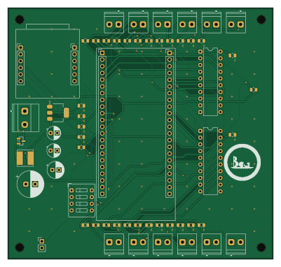
About the Baybasi panel PCB
Baybasi panel is an open source PCB design by riturajtiwari, published on GitHub under the MIT license. It is a 2-layer board measuring 100 × 95 mm, with 60 components from 19 distinct parts.
Other key parts include the SN74AHCT245N and AMS1117-3.3. By type, the board carries 27 resistors, 14 connectors, 9 capacitors, 4 modules, 3 ICs and 1 transistor.
It belongs with the displays & leds designs in this gallery.
From the project
WS2812B video wall: Raspberry Pi driver, upload utility, software DDP sink and ESP32-S3 controller firmware, with the KiCad board design
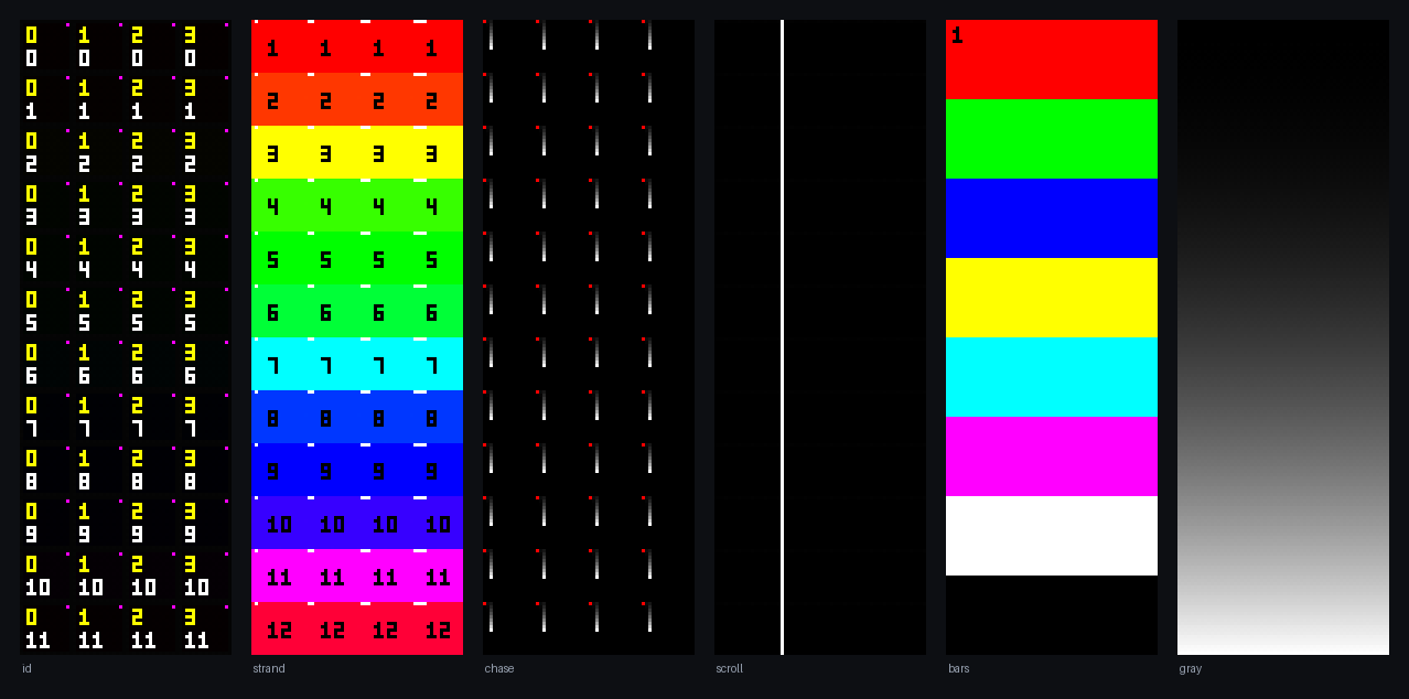
Software and firmware for a WS2812B video wall. The wall is 64 pixels wide and 192 pixels high. Each wall has 48 panels of 16 x 16 pixels.
There are two identical displays. The two displays do not share a cable, a ground or a clock. Each display is a complete and independent system.
The software runs today without hardware. A software DDP sink receives the pixel data and shows the result in a browser. You can test the driver and the upload utility before the boards arrive.
Main components on the Baybasi panel
Baybasi panel bill of materials (BOM)
60 components, 19 distinct parts — part numbers from the project's BOM.
| Qty | Part | Footprint | Refs |
|---|---|---|---|
| 2 | SN74AHCT245N DIP-20_W7.62mm | DIP-20_W7.62mm | U1, U2 |
| 1 | AMS1117-3.3 SOT-223-3_TabPin2 | SOT-223-3_TabPin2 | U3 |
| 2 | PinHeader_1x22_P2.54mm_Vertical | PinHeader_1x22_P2.54mm_Vertical | A1L, A1R |
| 2 | PinHeader_1x06_P2.54mm_Vertical | PinHeader_1x06_P2.54mm_Vertical | M1, M2 |
| 1 | AO3401A SOT-23 | SOT-23 | Q1 |
| 12 | TerminalBlock_Phoenix_PT-1,5-2-3.5-H_1x02_P3.50mm_Horizontal | TerminalBlock_Phoenix_PT-1,5-2-3.5-H_1x02_P3.50mm_Horizontal | J1, J2, J3, J4, J5, J6, J7, J8 +4 |
| 1 | TerminalBlock_Phoenix_MKDS-1,5-2-5.08_1x02_P5.08mm_Horizontal | TerminalBlock_Phoenix_MKDS-1,5-2-5.08_1x02_P5.08mm_Horizontal | J13 |
| 1 | PinHeader_1x02_P2.54mm_Vertical | PinHeader_1x02_P2.54mm_Vertical | J14 |
| 1 | SW_DIP_SPSTx04_Slide_9.78x12.34mm_W7.62mm_P2.54mm | SW_DIP_SPSTx04_Slide_9.78x12.34mm_W7.62mm_P2.54mm | SW1 |
| 1 | L_Bourns_SRN6045TA | L_Bourns_SRN6045TA | L1 |
| 1 | CP_Radial_D10.0mm_P3.50mm | CP_Radial_D10.0mm_P3.50mm | C1 |
| 1 | 100UF CP_Radial_D6.3mm_P2.50mm | CP_Radial_D6.3mm_P2.50mm | C2 |
| 1 | 10UF CP_Radial_D5.0mm_P2.50mm | CP_Radial_D5.0mm_P2.50mm | C3 |
| 1 | 22UF CP_Radial_D5.0mm_P2.50mm | CP_Radial_D5.0mm_P2.50mm | C4 |
| 5 | 100NF C_0805_2012Metric | C_0805_2012Metric | C5, C6, C7, C8, C9 |
| 12 | 330 R_0805_2012Metric | R_0805_2012Metric | R1, R2, R3, R4, R5, R6, R7, R8 +4 |
| 1 | 100K R_0805_2012Metric | R_0805_2012Metric | R13 |
| 2 | 10K R_0805_2012Metric | R_0805_2012Metric | R14, R15 |
| 12 | R_0805_2012Metric | R_0805_2012Metric | R16, R17, R18, R19, R20, R21, R22, R23 +4 |
Baybasi panel design files
The KiCad project lives in the riturajtiwari/baybasi-panel repository on GitHub; these links point at the commit this page was built from.
- Layouthw/baybasi-ctrl.kicad_pcb
- Schematichw/baybasi-ctrl.kicad_sch
- BOMhw/bom.csv
Baybasi panel: common questions
How big is the Baybasi panel PCB?
The Baybasi panel measures 100 × 95 mm, has 2 copper layers and is 1.6 mm thick.
How many components are on the Baybasi panel?
60 components, from 19 distinct parts, with part numbers taken from the project's own BOM. The full bill of materials is listed on this page.
Where can I download the Baybasi panel design files?
From the riturajtiwari/baybasi-panel repository on GitHub, which has the KiCad layout, the schematic and the BOM; the links under Design files point to each one.
Can I use the Baybasi panel design in my own project?
Yes, under the terms of its MIT license, which riturajtiwari chose for the repository.
Similar boards

LevelShifterBreakout
scottbez1
15.2 × 20.3 mm5 parts2LApache-2.022.2k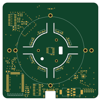
View base
81.2 × 81.2 mm81 parts2LApache-2.022.2k
View screen
35 × 35 mm12 parts2LApache-2.022.2k
BM28B0.6-24DSBreakout
15.2 × 35.6 mm3 parts2LApache-2.022.2k
ChainlinkDriverTester
198.1 × 95.3 mm123 parts2LApache-2.04.2k
ChainlinkBase
98.4 × 190.5 mm119 parts2LApache-2.04.2k