POWER NODE V2

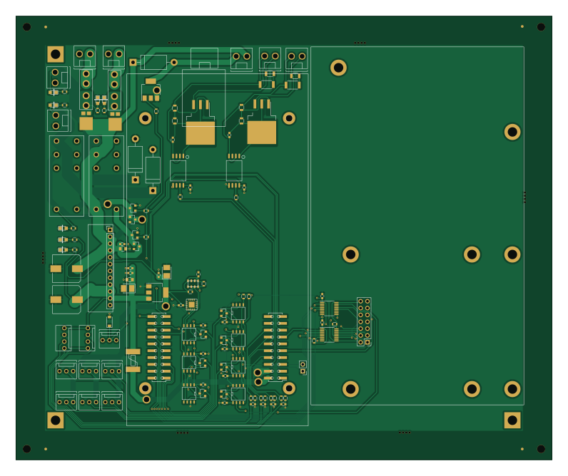
About the POWER NODE V2 PCB
POWER NODE V2 is an open source PCB design by rLoopTeam, published on GitHub. It is a 2-layer board measuring 198.8 × 164.8 mm, with 132 components from 53 distinct parts.
Other key parts include the LM1117MP-3.3/NOPB, R-745.0P, DS2482S-100+T&R, TSYS01 and MS5607-02BA03. By type, the board carries 34 resistors, 29 capacitors, 22 ICs, 22 connectors, 15 diodes and 7 transistors.
From the project
All PCB designs for rLoop in Altium Designer 13 format.
Altium Viewer License is needed: http://www.altium.com/altium-designer-viewer CAD files in Inventor 2013 format and .step.
Main components on the POWER NODE V2
POWER NODE V2 bill of materials (BOM)
132 components, 53 distinct parts — part numbers from the project's BOM.
| Qty | Part | Footprint | Refs |
|---|---|---|---|
| 1 | LM1117MP-3.3/NOPB | SOT-223 | U1 |
| 1 | R-745.0P | R-745.0P | U2 |
| 7 | DS2482S-100+T&R | SOIC-8-N | U3, U4, U5, U8, U9, U10, U11 |
| 1 | TSYS01 | QFN16_4x4 | U6 |
| 1 | MS5607-02BA03 | ms5607-02ba03 | U7 |
| 1 | NCV8405ADTRKG | SOT-223 | U12 |
| 2 | MAX14850AEE+ | QSOP-16_3.9x4.9mm_Pitch0.635mm | U13, U14 |
| 2 | TL783CKTTR | tl783ckttr | U15, U16 |
| 2 | AMC1100DWV | amc1100_SOIC8 | U17, U18 |
| 2 | NUD3124LT1G | SOT-23 | U19, U21 |
| 2 | RTE24024 | RTE24024 | U20, U22 |
| 7 | BSS84 | SOT-23 | Q1, Q2, Q3, Q4, Q5, Q6, Q7 |
| 7 | TE_3-641119-2 | 3-641119-2_TE_2P_MTA156_HDR | J1, J2, J9, J13, J14, J15, P1 |
| 2 | Keystone_3544-2 | Keystone_3544-2 | J3, J4 |
| 1 | 5-146130-9 | Booster1_Header_J1_J3 | J5 |
| 1 | 826926-2 | Pin_Header_Straight_1x02_Pitch2.54mm | J6 |
| 1 | 5-146130-9 | Booster1_J4_J2 | J7 |
| 7 | 3-641215-3 | 3-641215-3_3Pin_Latching_Header | J8, J16, J17, J18, J19, J20, J21 |
| 1 | 5-534998-7 | Pin_Header_Straight_2x07_Pitch2.54mm | J10 |
| 2 | CONN_01X04 | 22-04-1041_Molex_4_Pin_Header_2.50mm | J11, J12 |
Show 33 more
| Qty | Part | Footprint | Refs |
|---|---|---|---|
| 1 | 2920L300/15DR - 3A IH / 5A IT | 2920L300_15DR | F1 |
| 1 | RM57_Mounting_Holes | RM57_Mounting_Hole | RM57_Mounting_Holes |
| 1 | RM57_Launchpad_Outline | RM57_Launchpad_Outline | RM_57_Outline |
| 7 | EL-17-21VGC/TR8 | LED_0805 | D1, D2, D8, D10, D11, D12, D14 |
| 2 | FES10G | TO-277A_SMPC | D3, D4 |
| 1 | SMF6.5A / SOD-123 | D_SOD-123 | D5 |
| 1 | IN4004 | D_DO-201_P15.24mm_Horizontal | D6 |
| 2 | BAS16 | D_SOT-23_ANK | D7, D13 |
| 1 | 1N4004 | D_DO-201_P15.24mm_Horizontal | D9 |
| 1 | 1N4004 | 1N4004 | D15 |
| 2 | 330uF / 35V / 20% / SMD 10x10 | CP_Elec_10x10 | C1, C3 |
| 2 | 1uF / 50V / 10% / SMD 0805 | C_0805 | C2, C9 |
| 15 | 100n / 50V / 10% / SMD 0603 | C_0603 | C4, C5, C6, C7, C12, C13, C14, C15 +7 |
| 2 | 22uF / 16V / 10% / SMD TC3528 | CP_Tantalum_Case-T_EIA-3528-12_Reflow | C8, C10 |
| 4 | 200 nF / 50V / SMD 0603 | C_0603 | C23, C24, C25, C26 |
| 4 | 100nF / 50V / 10% / SMD 0603 | C_0603 | C27, C28, C29, C30 |
| 2 | 2.2K / 0.1W / 1% / SMD 0603 | R_0603 | R1, R2 |
| 1 | 2.2K / 0.1W / 10% / SMD 0603 | R_0603 | R3 |
| 1 | 500 / 0.1W / 10% / SMD 0603 | R_0603 | R4 |
| 1 | 300 / 0.1W / 10% / SMD 0603 | R_0603 | R5 |
| 4 | 4.7K / 0.1W / 1% / SMD 0603 | R_0603 | R6, R7, R8, R9 |
| 1 | 100 / .1W / 10% / SMD 0603 | R_0603 | R10 |
| 2 | 10K / .1W / 1% / SMD 0603 | R_0603 | R11, R12 |
| 2 | 300K / 0.5W / 1% / SMD 1206 | R_1206 | R13, R15 |
| 2 | 1K / 0.75W / 5% / 400V / SMD 2010 | R_2010 | R14, R16 |
| 4 | 2K / .1 W / 1% / SMD 0603 | R_0603 | R17, R18, R19, R20 |
| 4 | 10K / .1 W / 1% / SMD 0603 | R_0603 | R21, R22, R23, R24 |
| 2 | 82R0 / 0.25W / 1% / SMD 0805 | R_0805 | R25, R27 |
| 2 | 220R / 0.25W / 1% / SMD 0805 | R_0805 | R26, R28 |
| 2 | 50 / .1 W / 10% / SMD 0603 | R_0603 | R29, R33 |
| 2 | 1K0 / 0.063W / 1% / SMD 0603 | R_0603 | R30, R31 |
| 1 | 4.7k / .1 W / 10% / SMD 0603 | R_0603 | R32 |
| 1 | 4.7k / .1W / 10% / SMD 0603 | R_0603 | R34 |
POWER NODE V2 design files
The KiCad project lives in the rLoopTeam/elec-pcb repository on GitHub; these links point at the commit this page was built from.
POWER NODE V2: common questions
How big is the POWER NODE V2 PCB?
The POWER NODE V2 measures 198.8 × 164.8 mm, has 2 copper layers and is 1.6 mm thick.
How many components are on the POWER NODE V2?
132 components, from 53 distinct parts, with part numbers taken from the project's own BOM. The full bill of materials is listed on this page.
Where can I download the POWER NODE V2 design files?
From the rLoopTeam/elec-pcb repository on GitHub, which has the KiCad layout and the BOM; the links under Design files point to each one.
Can I use the POWER NODE V2 design in my own project?
The repository has no license, so all rights stay with rLoopTeam. Use it as a reference, and ask the author before reusing the design.