
Frankenstein foundation

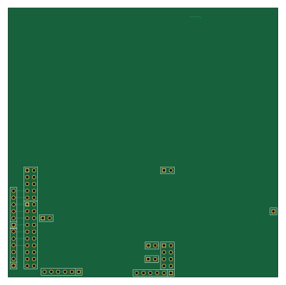
About the Frankenstein foundation PCB
Frankenstein foundation is an open source PCB design by rusefi, published on GitHub. It is a 2-layer board measuring 100 × 100 mm, with 14 components from 8 distinct parts.
By type, the board carries 9 connectors and 3 jumpers.
From the project
In this repo we archive rusEfi-related abandoned hardware files
Here we have hardware files related to things we have absolutely given up on just for the sake of history.
For more useful stuff see https://github.com/rusefi/rusefi/tree/master/hardware
Frankenstein foundation bill of materials (BOM)
14 components, 8 distinct parts — part numbers from the project's BOM.
| Qty | Part | Footprint | Refs |
|---|---|---|---|
| 1 | CONN_4X2 | pin_array_4x2 | P51 |
| 1 | CONN_10X2 | PIN_ARRAY_10X2_M | P52 |
| 1 | CONN_2 | PIN_ARRAY_2X1 | P53 |
| 1 | CONN_5X2 | PIN_ARRAY_5x2 | P54 |
| 4 | CONN_6 | PIN_ARRAY-6X1 | P55, P56, P57, P58 |
| 1 | CONN_1 | PIN_ARRAY_1 | P610 |
| 3 | JUMPER | PIN_ARRAY_2_A | JP51, JP52, JP53 |
| 2 | CONN_6 | PIN_ARRAY-6X1 | P_VOID1, P_VOID2 |
Frankenstein foundation design files
The KiCad project lives in the rusefi/hw_legacy repository on GitHub; these links point at the commit this page was built from.
Frankenstein foundation: common questions
How big is the Frankenstein foundation PCB?
The Frankenstein foundation measures 100 × 100 mm, has 2 copper layers and is 1.6 mm thick.
How many components are on the Frankenstein foundation?
14 components, from 8 distinct parts, with part numbers taken from the project's own BOM. The full bill of materials is listed on this page.
Where can I download the Frankenstein foundation design files?
From the rusefi/hw_legacy repository on GitHub, which has the KiCad layout and the BOM; the links under Design files point to each one.
Can I use the Frankenstein foundation design in my own project?
The repository has no license, so all rights stay with rusefi. Use it as a reference, and ask the author before reusing the design.
More boards in hw_legacy
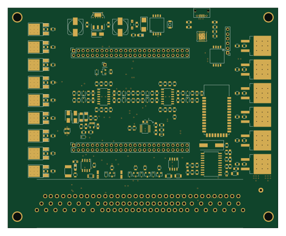
M52
145 × 118 mm226 parts2LNo license2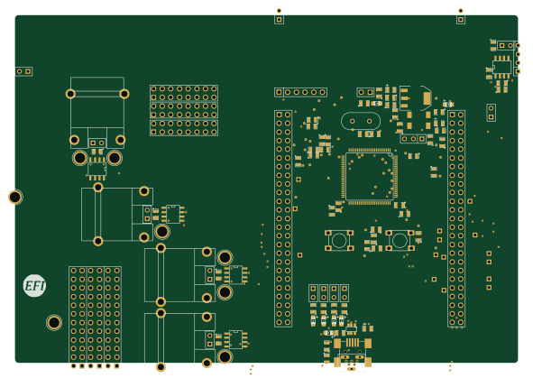 STM32
STM32Frankenso
147.6 × 102 mm127 parts2LNo license2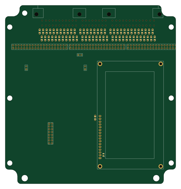
Frankenso foundation
154.1 × 161.7 mm75 parts2LNo license2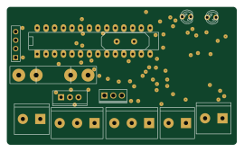 AVR/Arduino
WBO2
67.4 × 40.6 mm51 partsNo license2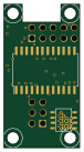
CJ125 Wide O2
18.2 × 34.3 mm39 parts2LNo license2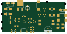
Ion
66 × 31.8 mm34 parts2LNo license2
Low Z injector driver
13.5 × 15.5 mm12 partsNo license2