
Crystal Test Circuit

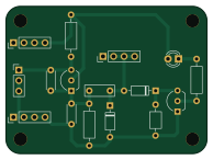
About the Crystal Test Circuit PCB
Crystal Test Circuit is an open source PCB design by sdp8483, published on GitHub under the MIT license. It is a 2-layer board measuring 48.5 × 35.6 mm, with 16 components from 10 distinct parts.
By type, the board carries 4 connectors, 4 capacitors, 3 diodes, 3 resistors and 2 transistors.
From the project
Various Test Circuits for all Projects
Directory structure for starting a basic project. Originally based off Hackaday article: https://hackaday.com/2017/05/18/kicad-best-practises-library-management/
Crystal Test Circuit bill of materials (BOM)
16 components, 10 distinct parts.
| Qty | Part | Footprint | Refs |
|---|---|---|---|
| 2 | Q_NPN_ECB | TO-92_Inline_Wide | Q1, Q2 |
| 3 | Conn_01x04 | PinHeader_1x04_P2.54mm_Vertical | J1, J2, J3 |
| 1 | xtal | PinHeader_1x03_P2.54mm_Vertical | J4 |
| 1 | LED | LED_D3.0mm | D1 |
| 2 | 1N4148 | D_DO-35_SOD27_P7.62mm_Horizontal | D2, D3 |
| 2 | 22pF | C_Disc_D4.3mm_W1.9mm_P5.00mm | C1, C2 |
| 1 | 1nF | C_Rect_L7.0mm_W2.5mm_P5.00mm | C3 |
| 1 | 100nF | C_Axial_L3.8mm_D2.6mm_P7.50mm_Horizontal | C4 |
| 1 | 33k | R_Axial_DIN0207_L6.3mm_D2.5mm_P10.16mm_Horizontal | R1 |
| 2 | 1k | R_Axial_DIN0207_L6.3mm_D2.5mm_P10.16mm_Horizontal | R2, R3 |
Crystal Test Circuit design files
The KiCad project lives in the sdp8483/pl_test_pcb repository on GitHub; these links point at the commit this page was built from.
Crystal Test Circuit: common questions
How big is the Crystal Test Circuit PCB?
The Crystal Test Circuit measures 48.5 × 35.6 mm, has 2 copper layers and is 1.6 mm thick.
How many components are on the Crystal Test Circuit?
16 components, from 10 distinct parts. The full bill of materials is listed on this page.
Where can I download the Crystal Test Circuit design files?
From the sdp8483/pl_test_pcb repository on GitHub, which has the KiCad layout and the schematic; the links under Design files point to each one.
Can I use the Crystal Test Circuit design in my own project?
Yes, under the terms of its MIT license, which sdp8483 chose for the repository.
More boards in pl_test_pcb
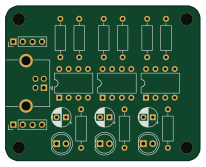
Tripple 555
51.5 × 41 mm21 parts2LMIT0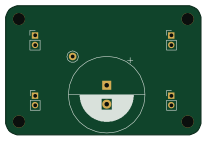
Super Capacitor Charge and Backup Circuit
51.6 × 34.1 mm20 parts2LMIT0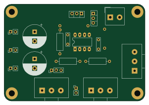
Opamp Motor Position Control
75.1 × 51.3 mm18 parts2LMIT0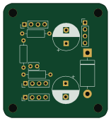
XL1410E1 Test
39 × 42.5 mm14 parts2LMIT0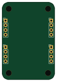
LGS5145 DCDC Converter Test Board
28.2 × 41.4 mm13 parts2LMIT0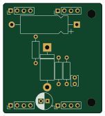
XL7005A Test
37.8 × 41.8 mm13 parts2LMIT0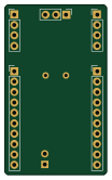 AVR/Arduino
Attiny416 breakout
25 × 41.4 mm9 parts2LMIT0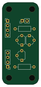
Constant Current Sink Test
19.4 × 43.9 mm8 parts2LMIT0
SSP7903 Test
32.9 × 8.2 mm7 parts2LMIT0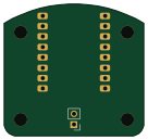 ESP32
ESP32Mini Christmas Tree Light Controller
34 × 32.2 mm5 parts2LMIT0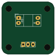
Photointerrupter Breakout
27 × 27 mm4 parts2LMIT0