
Tripple 555

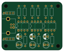
About the Tripple 555 PCB
Tripple 555 is an open source PCB design by sdp8483, published on GitHub under the MIT license. It is a 2-layer board measuring 51.5 × 41 mm, with 21 components from 8 distinct parts.
Other key parts include the NA555P. By type, the board carries 9 resistors, 3 ICs, 3 connectors, 3 diodes and 3 capacitors.
From the project
Various Test Circuits for all Projects
prototype circuits that dont warrent a seperate repo. Mostly undocumented, enter at your own risk!
Main components on the Tripple 555
Tripple 555 bill of materials (BOM)
21 components, 8 distinct parts.
| Qty | Part | Footprint | Refs |
|---|---|---|---|
| 3 | NA555P | DIP-8_W7.62mm | U1, U2, U3 |
| 2 | Conn_01x04 | PinHeader_1x04_P2.54mm_Vertical | J1, J2 |
| 1 | USB_B | USB_B_mill_spacing | J3 |
| 3 | LED | LED_D5.0mm | D1, D2, D3 |
| 3 | 10u | CP_Radial_D5.0mm_P2.50mm | C1, C2, C3 |
| 3 | 100k | R_Axial_DIN0207_L6.3mm_D2.5mm_P10.16mm_Horizontal | R1, R4, R7 |
| 3 | 470k | R_Axial_DIN0207_L6.3mm_D2.5mm_P10.16mm_Horizontal | R2, R5, R8 |
| 3 | 680 | R_Axial_DIN0207_L6.3mm_D2.5mm_P10.16mm_Horizontal | R3, R6, R9 |
Tripple 555 design files
The KiCad project lives in the sdp8483/pl_test_pcb repository on GitHub; these links point at the commit this page was built from.
Tripple 555: common questions
How big is the Tripple 555 PCB?
The Tripple 555 measures 51.5 × 41 mm, has 2 copper layers and is 1.6 mm thick.
How many components are on the Tripple 555?
21 components, from 8 distinct parts. The full bill of materials is listed on this page.
Where can I download the Tripple 555 design files?
From the sdp8483/pl_test_pcb repository on GitHub, which has the KiCad layout and the schematic; the links under Design files point to each one.
Can I use the Tripple 555 design in my own project?
Yes, under the terms of its MIT license, which sdp8483 chose for the repository.
More boards in pl_test_pcb
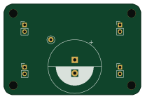
Super Capacitor Charge and Backup Circuit
51.6 × 34.1 mm20 parts2LMIT0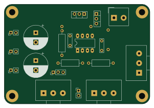
Opamp Motor Position Control
75.1 × 51.3 mm18 parts2LMIT0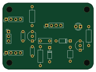
Crystal Test Circuit
48.5 × 35.6 mm16 parts2LMIT0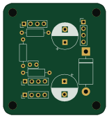
XL1410E1 Test
39 × 42.5 mm14 parts2LMIT0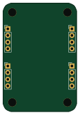
LGS5145 DCDC Converter Test Board
28.2 × 41.4 mm13 parts2LMIT0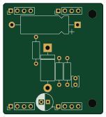
XL7005A Test
37.8 × 41.8 mm13 parts2LMIT0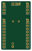 AVR/Arduino
Attiny416 breakout
25 × 41.4 mm9 parts2LMIT0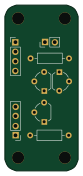
Constant Current Sink Test
19.4 × 43.9 mm8 parts2LMIT0
SSP7903 Test
32.9 × 8.2 mm7 parts2LMIT0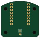 ESP32
ESP32Mini Christmas Tree Light Controller
34 × 32.2 mm5 parts2LMIT0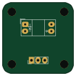
Photointerrupter Breakout
27 × 27 mm4 parts2LMIT0