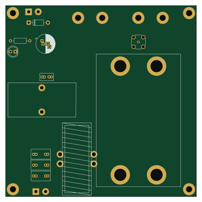
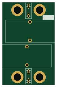
Switching network

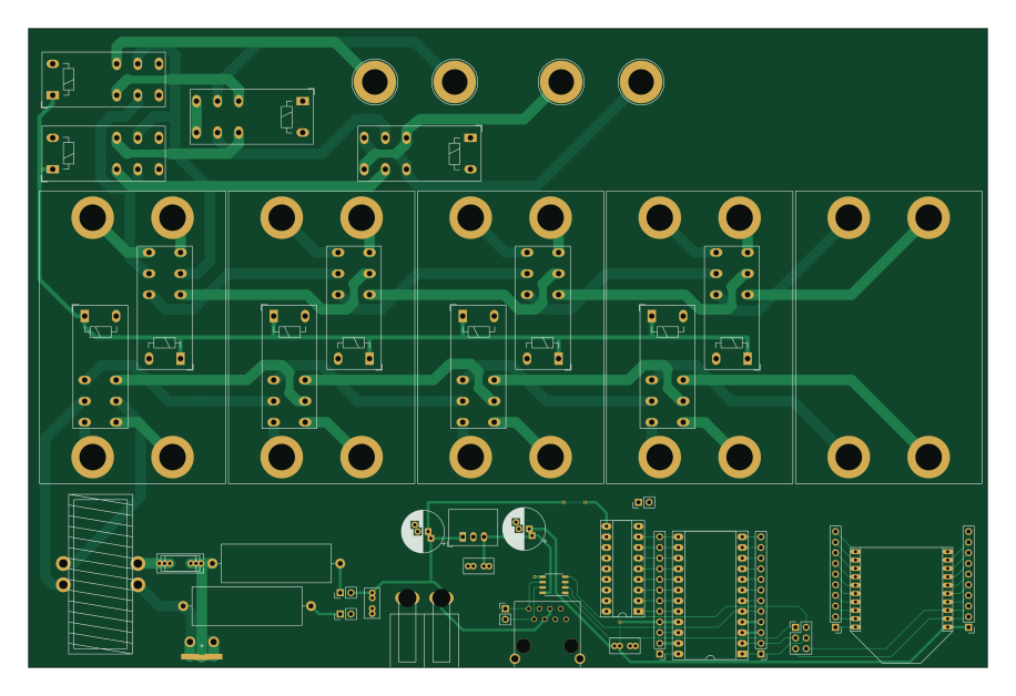
About the Switching network PCB
Switching network is an open source PCB design by SmittyHalibut, published on GitHub. It is a 2-layer board measuring 228.6 × 152.4 mm, with 49 components from 35 distinct parts.
Other key parts include the SN65HVD10-EP, XBeeModule, R-783.3-0.5, Leonardo_Pro_Micro and ULN2803A. By type, the board carries 19 connectors, 12 relays, 8 capacitors, 5 ICs, 3 inductors and 2 jumpers.
From the project
Notes and files for my BayCon 2021 presentation Raw data, and analysis of data, from NanoVNA Saver of my build of this antenna. Diagram for full switching network OpenSCAD and .stl files for my top-of-mast spreader bracket
Main components on the Switching network
Switching network bill of materials (BOM)
49 components, 35 distinct parts.
| Qty | Part | Footprint | Refs |
|---|---|---|---|
| 1 | SN65HVD10-EP | SOIC-8_3.9x4.9mm_P1.27mm | U1 |
| 1 | XBeeModule | XBeeModule | U2 |
| 1 | R-783.3-0.5 | Converter_DCDC_RECOM_R-78E-0.5_THT | U3 |
| 1 | Leonardo_Pro_Micro | DIP-24_W15.24mm_Socket_LongPads | U4 |
| 1 | ULN2803A | DIP-18_W7.62mm_Socket_LongPads | U5 |
| 1 | Conn_Coaxial | SMA_Samtec_SMA-J-P-H-ST-EM1_EdgeMount | J1 |
| 1 | Module 1 Socket | MatchingNetworkModule | J3 |
| 1 | Module 2 Socket | MatchingNetworkModule | J4 |
| 1 | Module 3 Socket | MatchingNetworkModule | J5 |
| 1 | Module 4 Socket | MatchingNetworkModule | J6 |
| 1 | Module 5 Socket | MatchingNetworkModule | J7 |
| 1 | NS+ | Banana_Jack_1Pin | J8 |
| 1 | Simple Bias Tee Rotation Control | PinHeader_1x02_P2.54mm_Vertical | J9 |
| 1 | NS- | Banana_Jack_1Pin | J10 |
| 1 | 8P8C_Shielded | RJ-45 | J11 |
| 2 | Test Points | PinHeader_1x10_P2.54mm_Vertical | J12, J15 |
| 1 | Test Points | PinHeader_1x02_P2.54mm_Vertical | J13 |
| 1 | RS-485 vs XBee | PinHeader_2x03_P2.54mm_Vertical | J14 |
| 2 | Test Points | PinHeader_1x12_P2.54mm_Vertical | J16, J17 |
| 1 | EW+ | Banana_Jack_1Pin | J18 |
Show 15 more
| Qty | Part | Footprint | Refs |
|---|---|---|---|
| 1 | EW- | Banana_Jack_1Pin | J19 |
| 1 | +12v Power | AndersonPP45 | J20 |
| 2 | Jumper_NC_Small | PinHeader_1x02_P2.54mm_Vertical | JP1, JP2 |
| 8 | RT42xxxx | Relay_DPDT_Schrack-RT2-FormC_RM5mm | K1, K2, K3, K4, K5, K6, K7, K8 |
| 1 | N/S Disable | Relay_DPDT_Schrack-RT2-FormC_RM5mm | K9 |
| 1 | E/W Disable | Relay_DPDT_Schrack-RT2-FormC_RM5mm | K10 |
| 1 | Series Enable | Relay_DPDT_Schrack-RT2-FormC_RM5mm | K11 |
| 1 | E/W Reverse | Relay_DPDT_Schrack-RT2-FormC_RM5mm | K12 |
| 1 | 1:1 Balun | Balun-FT140 | L1 |
| 2 | RF Choke | L_Axial_L26.0mm_D9.0mm_P30.48mm_Horizontal_Fastron_77A | L2, L3 |
| 1 | .1uF | C_Rect_L7.0mm_W3.5mm_P5.00mm | C1 |
| 3 | .1uF | C_Rect_L7.0mm_W3.5mm_P2.50mm_P5.00mm | C2, C5, C6 |
| 2 | 100uF | CP_Radial_D10.0mm_P2.50mm_P5.00mm | C3, C4 |
| 1 | .1uF | C_Rect_L9.0mm_W3.6mm_P7.50mm_MKT | C7 |
| 1 | .1uF | C_Rect_L11.0mm_W4.3mm_P10.00mm_MKT | C8 |
Switching network design files
The KiCad project lives in the SmittyHalibut/DoubleDeltaSlotAntenna repository on GitHub; these links point at the commit this page was built from.
Switching network: common questions
How big is the Switching network PCB?
The Switching network measures 228.6 × 152.4 mm, has 2 copper layers and is 1.6 mm thick.
How many components are on the Switching network?
49 components, from 35 distinct parts. The full bill of materials is listed on this page.
Where can I download the Switching network design files?
From the SmittyHalibut/DoubleDeltaSlotAntenna repository on GitHub, which has the KiCad layout; the links under Design files point to each one.
Can I use the Switching network design in my own project?
The repository has no license, so all rights stay with SmittyHalibut. Use it as a reference, and ask the author before reusing the design.