
Fatotesa KDB

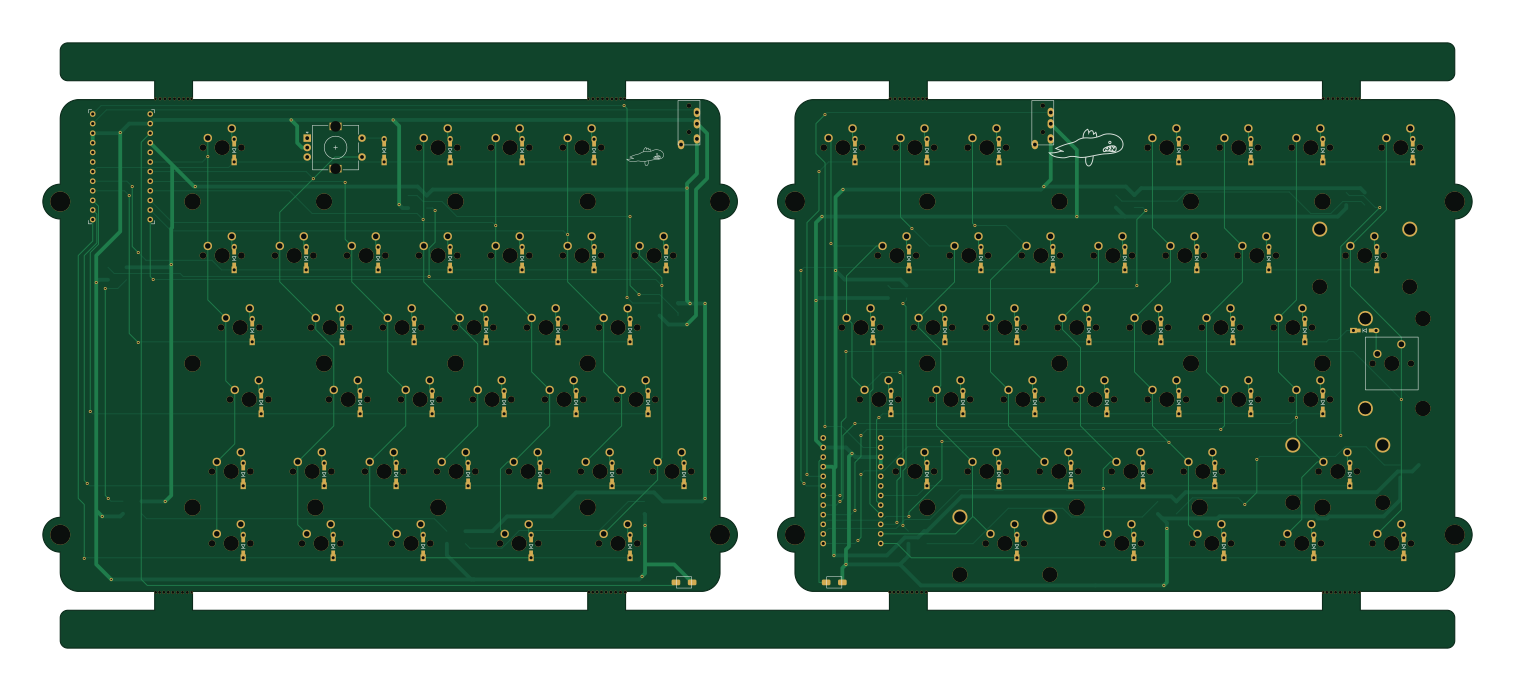
About the Fatotesa KDB PCB
Fatotesa KDB is an open source PCB design by stefangluszek, published on GitHub. It is a 2-layer board measuring 378.3 × 160.2 mm, with 182 components from 14 distinct parts.
Other key parts include the ProMicro. By type, the board carries 86 LEDs, 7 switches, 2 ICs and 2 connectors.
It belongs with the keyboards designs in this gallery.
From the project
The requirements I had were simple, a split mechanical keyboard with the base layout as close to the ISO layout as possible to make switching back and forth as painless as possible. Why ISO? Because I use a Swedish/Norwegian keyboard which uses the ISO layout.
The requirements I had were simple, a split mechanical keyboard with the base layout as close to the ISO layout as possible to make switching back and forth as painless as possible. Why ISO? Because I use a Swedish/Norwegian keyboard which uses the ISO layout.
The PCB routing and component placement is also improved. All signal traces are routed on the bottom layer and the top layer is used as a ground layer. Since this is a keyboard matrix, I had to use some vias to jump over the vertical traces when routing the horizontal ones. An alternative, which most other keyboards seem to go for, is…
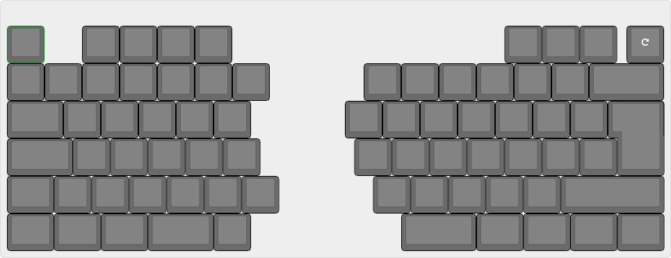
Main components on the Fatotesa KDB
Fatotesa KDB bill of materials (BOM)
182 components, 14 distinct parts — part numbers from the project's BOM.
| Qty | Part | Footprint | Refs |
|---|---|---|---|
| 2 | ProMicro | ProMicro_v3_inverted | U1, U3 |
| 2 | MJ-4PP-9 | MJ-4PP-9_1side | J1, J2 |
| 76 | D | D3_TH | D_0, D_1, D_2, D_3, D_4, D_5, D_6, D_7 +68 |
| 8 | MountingHole | breakaway-mousebites_fat-o-tesa | H33, H34, H35, H36, H37, H38, H39, H40 |
| 1 | KEYSW | SW_Cherry_MX_ISOEnter_PCB | K_73 |
| 3 | MX_stab | STAB_MX_P_2u | S1, S3, S4 |
| 1 | MX_stab | STAB_MX_P_2.75u | S2 |
| 2 | SW_PUSH | ResetSMD_SG | SW1, SW2 |
| 1 | RotaryEncoder_Switch | RotaryEncoder_Alps_EC11E-Switch_Vertical_H20mm | SW3 |
| 63 | KEYSW | MXOnly-1U-NoLED | K_0, K_1, K_2, K_3, K_4, K_5, K_6, K_7 +55 |
| 1 | KEYSW | MXOnly-1.5U-NoLED | K_11 |
| 2 | KEYSW | MXOnly-1.75U-NoLED | K_17, K_33 |
| 8 | KEYSW | MXOnly-1.25U-NoLED | K_23, K_30, K_31, K_32, K_56, K_62, K_67, K_74 |
| 12 | WS2812B | LED_WS2812B_PLCC4_5.0x5.0mm_P3.2mm | LED1, LED2, LED3, LED4, LED5, LED6, LED7, LED8 +4 |
Fatotesa KDB design files
The KiCad project lives in the stefangluszek/fat-o-tesa repository on GitHub; these links point at the commit this page was built from.
Fatotesa KDB: common questions
How big is the Fatotesa KDB PCB?
The Fatotesa KDB measures 378.3 × 160.2 mm, has 2 copper layers and is 1.6 mm thick.
How many components are on the Fatotesa KDB?
182 components, from 14 distinct parts, with part numbers taken from the project's own BOM. The full bill of materials is listed on this page.
Where can I download the Fatotesa KDB design files?
From the stefangluszek/fat-o-tesa repository on GitHub, which has the KiCad layout, the schematic and the BOM; the links under Design files point to each one.
Can I use the Fatotesa KDB design in my own project?
The repository has no license, so all rights stay with stefangluszek. Use it as a reference, and ask the author before reusing the design.
More boards in fat-o-tesa
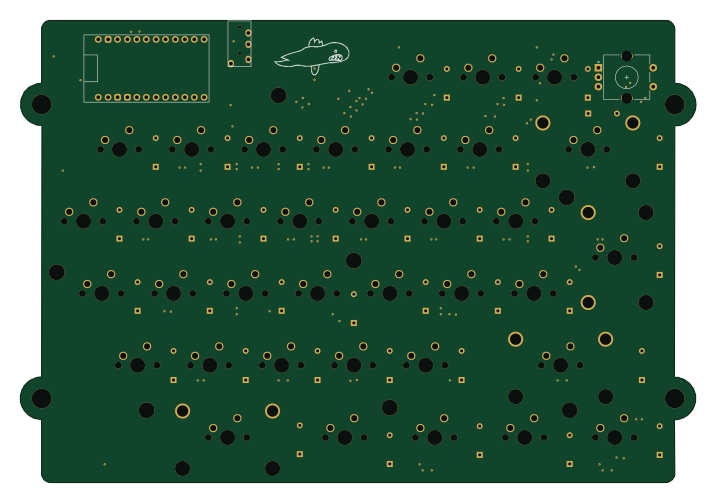
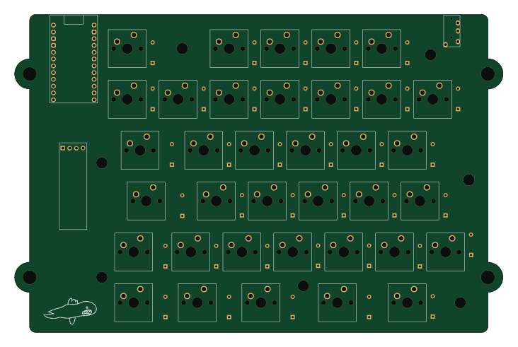
Similar boards
Lily58 Lite Rev3 TOP Case
kata0510
142.5 × 106.4 mm34 parts2LMIT2.3k
Lily58 Pro BOTTOM
142.5 × 106.3 mm5 parts2LMIT2.3k
Lily58
142.5 × 106.3 mm83 parts2LMIT2.3k
Lily58 Pro
142.5 × 106.3 mm83 parts2LMIT2.3k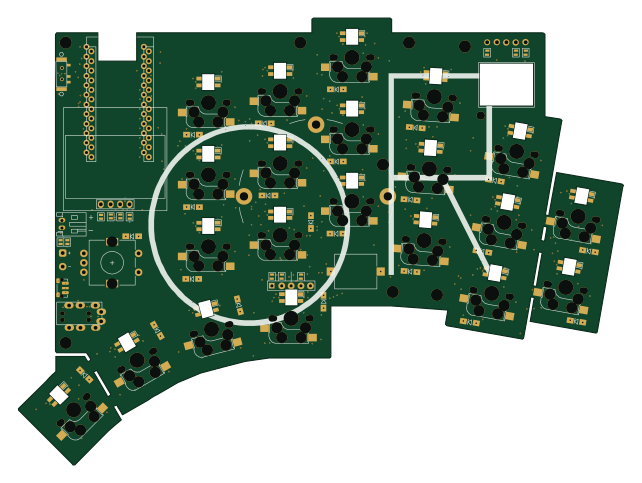
KLOR
GEIGEIGEIST
160.2 × 118.3 mm79 parts2LGPL-3.01.2k
Pcb top
tompi
132.5 × 95.1 mm18 parts2LCC-BY-4.01.2k