
Windows ai eda workflow

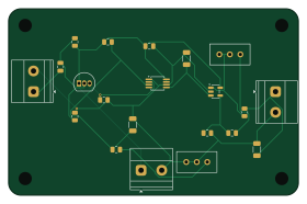
About the Windows ai eda workflow PCB
Windows ai eda workflow is an open source PCB design by sutony1, published on GitHub under the MIT license. It is a 2-layer board measuring 70 × 45 mm, with 21 components from 18 distinct parts.
Other key parts include the LTC1967CMS8 and OPA333AIDBVR. By type, the board carries 8 resistors, 5 capacitors, 3 connectors, 2 ICs and 1 transistor.
From the project
Reproducible Windows SPICE to KiCad 10 to EasyEDA/JLCPCB workflow with Codex skills
Target: 0–300 mVrms, 50 Hz current-transformer voltage input to approximately 0–3 V DC from a 5 V supply.
- kicad/: authoritative KiCad 10 schematic, project, and routed PCB. - simulation/: ngspice behavioural smoke test, portable LTspice sweep deck, and measured simulation results. - hardware-test/: PyVISA/RIGOL automated verification example. - manufacturing/: checked Gerber ZIP plus BOM and pick-and-place CSV.
Main components on the Windows ai eda workflow
Windows ai eda workflow bill of materials (BOM)
21 components, 18 distinct parts — part numbers from the project's BOM.
| Qty | Part | Footprint | Refs |
|---|---|---|---|
| 1 | LTC1967CMS8 | MSOP-8_3x3mm_P0.65mm | U1 |
| 1 | OPA333AIDBVR | SOT-23-5 | U2 |
| 1 | BC547B | TO-92_Inline | Q1 |
| 1 | CT IN 0-300mVrms | TerminalBlock_Phoenix_MKDS-1,5-2_1x02_P5.00mm_Horizontal | J1 |
| 1 | OUT 0-3V DC | TerminalBlock_Phoenix_MKDS-1,5-2_1x02_P5.00mm_Horizontal | J2 |
| 1 | +5V / GND | TerminalBlock_Phoenix_MKDS-1,5-2_1x02_P5.00mm_Horizontal | J3 |
| 1 | 10k trim (set 5.1k) | Potentiometer_Bourns_3296W_Vertical | RV1 |
| 1 | 5k trim (set 0.44k) | Potentiometer_Bourns_3296W_Vertical | RV2 |
| 1 | 1UF 1uF | C_0805_2012Metric | C1 |
| 2 | 10UF 10uF | C_1206_3216Metric | C2, C4 |
| 1 | 100NF 100nF | C_0805_2012Metric | C5 |
| 1 | 10uF RMS average | C_1206_3216Metric | C6 |
| 3 | 47K 47k | R_0805_2012Metric | R1, R2, R4 |
| 1 | 10K 10k | R_0805_2012Metric | R3 |
| 1 | 22k 1% | R_0805_2012Metric | R5 |
| 1 | 10k 0.1% | R_0805_2012Metric | R6 |
| 1 | 93.1k 0.1% | R_0805_2012Metric | R7 |
| 1 | 1k | R_0805_2012Metric | R8 |
Windows ai eda workflow design files
The KiCad project lives in the sutony1/windows-ai-eda-workflow repository on GitHub; these links point at the commit this page was built from.
Windows ai eda workflow: common questions
How big is the Windows ai eda workflow PCB?
The Windows ai eda workflow measures 70 × 45 mm, has 2 copper layers and is 1.6 mm thick.
How many components are on the Windows ai eda workflow?
21 components, from 18 distinct parts, with part numbers taken from the project's own BOM. The full bill of materials is listed on this page.
Where can I download the Windows ai eda workflow design files?
From the sutony1/windows-ai-eda-workflow repository on GitHub, which has the KiCad layout, the schematic and the BOM; the links under Design files point to each one.
Can I use the Windows ai eda workflow design in my own project?
Yes, under the terms of its MIT license, which sutony1 chose for the repository.