
LargePW

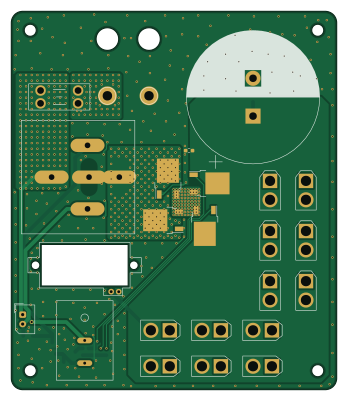
About the LargePW PCB
LargePW is an open source PCB design by Tomoshibi-technology, published on GitHub under the MIT license. It is a 2-layer board measuring 86 × 100 mm, with 36 components from 16 distinct parts.
By type, the board carries 13 connectors, 7 resistors, 6 transistors, 2 diodes, 2 capacitors and 1 fuse.
From the project
RoboCup JapanOpen 2024とEindohoven 2024に向けての回路開発
LargePW bill of materials (BOM)
36 components, 16 distinct parts — part numbers from the project's BOM.
| Qty | Part | Footprint | Refs |
|---|---|---|---|
| 4 | TJ60S04M3L | TO-252-2 | Q1, Q2, Q3, Q4 |
| 2 | BSS138 | SOT-23_Handsoldering | Q5, Q6 |
| 1 | CONN_01X02_FEMALE Conn_01x02_Female | Molex_SPOX_5267-02A_1x02_P2.50mm_Vertical | J1 |
| 12 | CONN_01X02_FEMALE Conn_01x02_Female | AMASS_XT30U-F_1x02_P5.0mm_Vertical | J2, J3, J4, J5, J6, J7, J8, J9 +4 |
| 1 | Fuse | Fuseholder_Blade_Mini_Keystone_3568 | F1 |
| 2 | MountingHole_Pad | TestPoint_THTPad_D4.0mm_Drill2.0mm | H1, H2 |
| 1 | RAYEX-L90 | TRV4-L-12V-Z-F | K1 |
| 1 | Voltmeter_DC | SuperSmallVoltmeter_twoline | MES1 |
| 1 | SW_SPST | DS-850K-S-ON | SW1 |
| 2 | CUS10F30 | D_SOD-323_HandSoldering | D1, D2 |
| 1 | 1UF 1uF | C_0603_1608Metric_Pad1.08x0.95mm_HandSolder | C1 |
| 1 | 10000UF 10000uF | CP_Radial_D35.0mm_P10.00mm_SnapIn | C2 |
| 3 | 10K 10k | R_0603_1608Metric_Pad0.98x0.95mm_HandSolder | R1, R5, R6 |
| 1 | 100K 100k | R_0603_1608Metric_Pad0.98x0.95mm_HandSolder | R2 |
| 2 | 510 | R_0603_1608Metric_Pad0.98x0.95mm_HandSolder | R3, R4 |
| 1 | 1k | R_0603_1608Metric_Pad0.98x0.95mm_HandSolder | R7 |
LargePW design files
The KiCad project lives in the Tomoshibi-technology/RCJ-Japan2024-Circuit repository on GitHub; these links point at the commit this page was built from.
LargePW: common questions
How big is the LargePW PCB?
The LargePW measures 86 × 100 mm, has 2 copper layers and is 1.6 mm thick.
How many components are on the LargePW?
36 components, from 16 distinct parts, with part numbers taken from the project's own BOM. The full bill of materials is listed on this page.
Where can I download the LargePW design files?
From the Tomoshibi-technology/RCJ-Japan2024-Circuit repository on GitHub, which has the KiCad layout, the schematic and the BOM; the links under Design files point to each one.
Can I use the LargePW design in my own project?
Yes, under the terms of its MIT license, which Tomoshibi-technology chose for the repository.
More boards in RCJ-Japan2024-Circuit
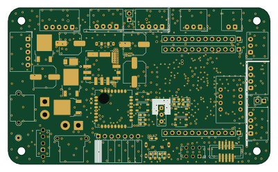 STM32
STM32Mother Ctrl
100 × 60 mm248 parts2LMIT1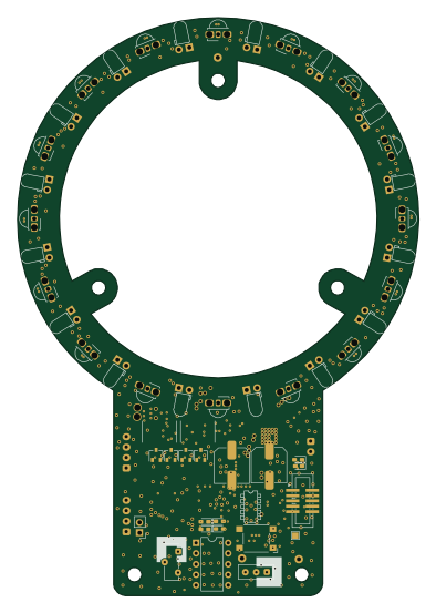 STM32
STM32IR
96 × 138 mm190 parts2LMIT1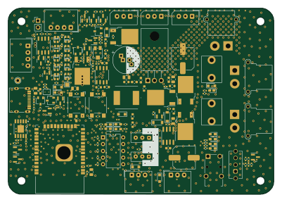 ESP32
ESP32Pole
100 × 70 mm181 parts2LMIT1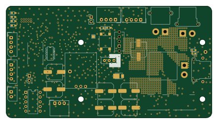 STM32
STM32LargeMD
110 × 60 mm148 parts2LMIT1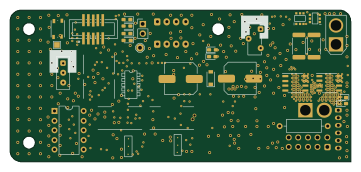 STM32
STM32SmallMD
90 × 40 mm142 parts2LMIT1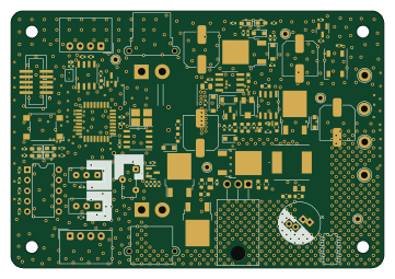 STM32
STM32Panel
90 × 62 mm118 parts2LMIT1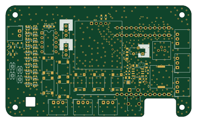
Mother UI
100 × 60 mm92 parts2LMIT1 STM32
STM32Encoder
50 × 40 mm57 parts2LMIT1
LED lighting large
94 × 94 mm34 parts2LMIT1
SmallPW
76 × 40 mm18 parts2LMIT1