
Mezzanine

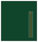
About the Mezzanine PCB
Mezzanine is an open source PCB design by wafer-space, published on GitHub under the Apache-2.0 license. It is a 2-layer board measuring 33.5 × 37.5 mm, with 9 components from 9 distinct parts.
Other key parts include the Caravel_COB. By type, the board carries 5 connectors and 4 ICs.
From the project
Wire bonded chip on board PCB designs.
Over the past few weeks we have been considering a number of different designs.
There are some projects that require a high pin count. In an effort to keep prices down and use components that are widely available the current highest choice option seems to be an LGA (Land Grid Array). The current version has 100 user pins--even though the default pad frame will contain only 73 wire bonds this will enable extra ground and power pads for analog and other signals that benefit from close proximity.
Main components on the Mezzanine
Mezzanine bill of materials (BOM)
9 components, 9 distinct parts — part numbers from the project's BOM.
| Qty | Part | Footprint | Refs |
|---|---|---|---|
| 1 | Caravel_COB | waferspace_default_padring_v0 | U101 |
| 1 | Caravel_COB | caravel_gfmpw_1_0_asap | U102 |
| 1 | Caravel_COB | LGA2 | U103 |
| 1 | Caravel_COB | LGA1 | U104 |
| 1 | Conn_02x35_Counter_Clockwise_MountingPin | CONN-SMD_70P-P0.40_HCTL_HC-PBB40C-70DP-0.4V-02 | J101 |
| 1 | Conn_2Rows-76Pins | waferspace_default_padring_v0.1 | J102 |
| 1 | Conn_02x20_Counter_Clockwise_MountingPin | CONN-SMD_YXT-BB10-50S-02 | J103 |
| 1 | Conn_02x20_Counter_Clockwise_MountingPin | CONN-SMD_YXT-BB10-40S-02 | J104 |
| 1 | Conn_02x10_Odd_Even | PinHeader_2x19_P1.27mm_Vertical | J105 |
Mezzanine design files
The KiCad project lives in the wafer-space/chip-on-board-wire-bonded-pcbs repository on GitHub; these links point at the commit this page was built from.
Mezzanine: common questions
How big is the Mezzanine PCB?
The Mezzanine measures 33.5 × 37.5 mm, has 2 copper layers and is 1.6 mm thick.
How many components are on the Mezzanine?
9 components, from 9 distinct parts, with part numbers taken from the project's own BOM. The full bill of materials is listed on this page.
Where can I download the Mezzanine design files?
From the wafer-space/chip-on-board-wire-bonded-pcbs repository on GitHub, which has the KiCad layout, the schematic and the BOM; the links under Design files point to each one.
Can I use the Mezzanine design in my own project?
Yes, under the terms of its Apache-2.0 license, which wafer-space chose for the repository.
More boards in chip-on-board-wire-bonded-pcbs

Untitled
12.5 × 11.9 mm420 parts4LApache-2.012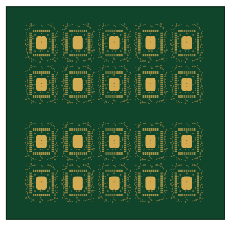
Panel
84 × 82 mm20 parts4LApache-2.012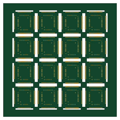
Waferspace cob
100 × 100 mm12 parts2LApache-2.012
Mezzanine-0p5x1
14 × 16 mm10 parts2LApache-2.012
Mezzanine-1x0p5
14 × 16 mm10 parts2LApache-2.012
1x1-mezzanine
14 × 16 mm9 parts4LApache-2.012
0p5x0p5-cob
14 × 16 mm6 parts2LApache-2.012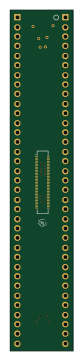
Motherboards
16.5 × 90.2 mm6 parts2LApache-2.012
Tqva cob
14 × 16 mm6 parts2LApache-2.012