
Tqva cob


About the Tqva cob PCB
Tqva cob is an open source PCB design by wafer-space, published on GitHub under the Apache-2.0 license. It is a 2-layer board measuring 14 × 16 mm, with 6 components from 3 distinct parts.
By type, the board carries 4 capacitors and 2 ICs.
From the project
Wire bonded chip on board PCB designs.
This directory holds the design files for Run 1 of the wafer.space chip-on-board (COB) breakouts.
Our current padframe and wirebonding layouts follow the Tiny Tapeout convention of 74 pads. All ground (GND) connections are tied together in the Default Breakout COB package.
Space has been allocated for optional components such as decoupling capacitors and other passive elements.
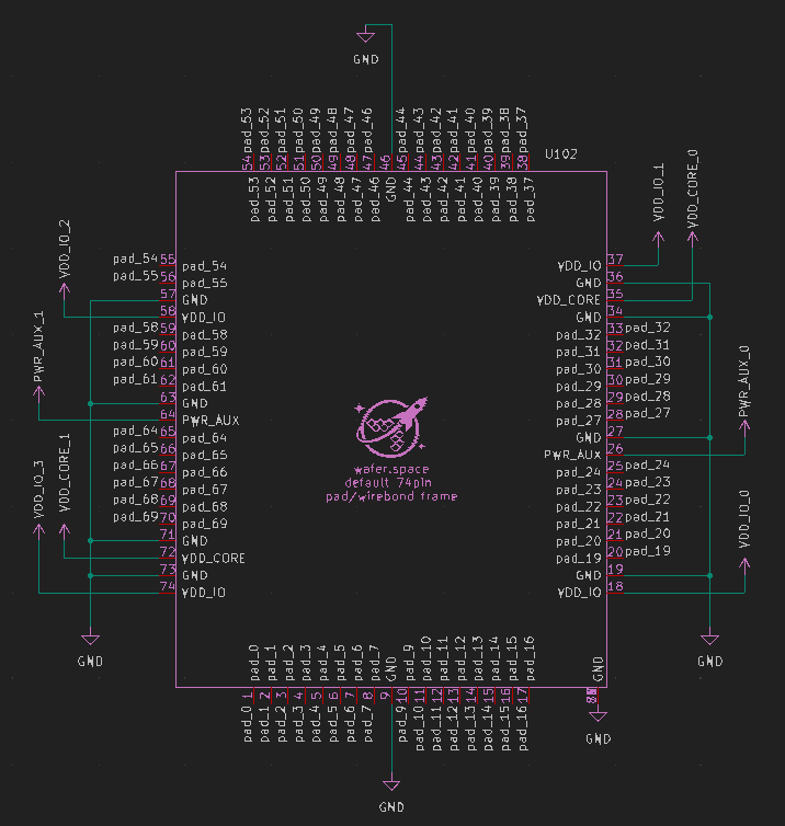
Tqva cob bill of materials (BOM)
6 components, 3 distinct parts — part numbers from the project's BOM.
| Qty | Part | Footprint | Refs |
|---|---|---|---|
| 1 | ~ | CONN-SMD_70P-P0.40_HCTL_HC-PBB40C-70DP-0.4V-02 | U101 |
| 1 | ~ | waferspace_p5xp5_padring | U102 |
| 4 | C_Small | C_0201_0603Metric | C101, C102, C104, C108 |
Tqva cob design files
The KiCad project lives in the wafer-space/chip-on-board-wire-bonded-pcbs repository on GitHub; these links point at the commit this page was built from.
Tqva cob: common questions
How big is the Tqva cob PCB?
The Tqva cob measures 14 × 16 mm, has 2 copper layers and is 1.6 mm thick.
How many components are on the Tqva cob?
6 components, from 3 distinct parts, with part numbers taken from the project's own BOM. The full bill of materials is listed on this page.
Where can I download the Tqva cob design files?
From the wafer-space/chip-on-board-wire-bonded-pcbs repository on GitHub, which has the KiCad layout, the schematic and the BOM; the links under Design files point to each one.
Can I use the Tqva cob design in my own project?
Yes, under the terms of its Apache-2.0 license, which wafer-space chose for the repository.
More boards in chip-on-board-wire-bonded-pcbs

Untitled
12.5 × 11.9 mm420 parts4LApache-2.012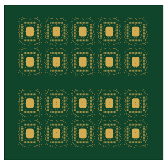
Panel
84 × 82 mm20 parts4LApache-2.012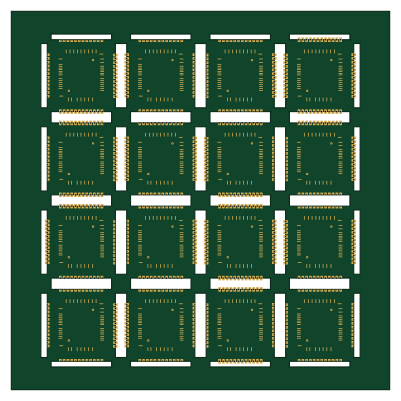
Waferspace cob
100 × 100 mm12 parts2LApache-2.012
Mezzanine-1x0p5
14 × 16 mm10 parts2LApache-2.012
Mezzanine-0p5x1
14 × 16 mm10 parts2LApache-2.012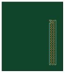
Mezzanine
33.5 × 37.5 mm9 parts2LApache-2.012
1x1-mezzanine
14 × 16 mm9 parts4LApache-2.012
0p5x0p5-cob
14 × 16 mm6 parts2LApache-2.012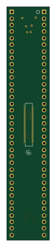
Motherboards
16.5 × 90.2 mm6 parts2LApache-2.012