
Jacks

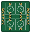
About the Jacks PCB
Jacks is an open source PCB design by wntrblm, published on GitHub under the CC-BY-SA-4.0 license. It is a 2-layer board measuring 26.7 × 27.9 mm, with 6 components from 6 distinct parts.
From the project
Re-usable test jig controller
Hubble is Winterbloom's re-usable development board for test jigs.
This repository contains the hardware design files and firmware files for Hubble.
- firmware/ contains the firmware source code, build scripts, and third-party dependencies. The firmware is written in C using GCC ARM. - hardware/ contains the hardware design files for the mainboard, jackboard, panel, and programming board. These are all created using KiCAD. - mechanical/ contains various designs for laser-cut and 3d-printed parts used to modify the stock test jig assembly for Hubble.
Jacks bill of materials (BOM)
6 components, 6 distinct parts.
| Qty | Part | Footprint | Refs |
|---|---|---|---|
| 1 | Left | PinSocket_1x06_P2.54mm_Vertical | J1 |
| 1 | A | WQP-WQP518MA | J2 |
| 1 | B | WQP-WQP518MA | J3 |
| 1 | C | WQP-WQP518MA | J4 |
| 1 | D | WQP-WQP518MA | J5 |
| 1 | Right | PinSocket_1x06_P2.54mm_Vertical | J6 |
Jacks design files
The KiCad project lives in the wntrblm/Hubble repository on GitHub; these links point at the commit this page was built from.
Jacks: common questions
How big is the Jacks PCB?
The Jacks measures 26.7 × 27.9 mm, has 2 copper layers and is 1.6 mm thick.
How many components are on the Jacks?
6 components, from 6 distinct parts. The full bill of materials is listed on this page.
Where can I download the Jacks design files?
From the wntrblm/Hubble repository on GitHub, which has the KiCad layout; the links under Design files point to each one.
Can I use the Jacks design in my own project?
Yes, under the terms of its CC-BY-SA-4.0 license, which wntrblm chose for the repository.
More boards in Hubble
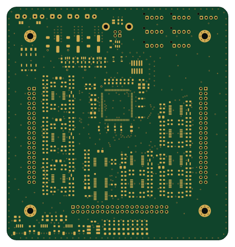 Microchip SAM
Hubble Motherboard
114 × 120 mm320 parts4LCC-BY-SA-4.023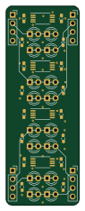
Leds
21.6 × 58.4 mm40 parts2LCC-BY-SA-4.023
TestKit Adapter Template
100 × 100 mm35 parts2LCC-BY-SA-4.023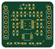
12-bit analog outputs
27.1 × 24 mm30 parts2LCC-BY-SA-4.023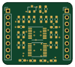
16 bit analog out
27.1 × 24 mm29 parts2LCC-BY-SA-4.023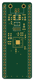 Microchip SAM
Mcu
26.9 × 68.6 mm27 parts2LCC-BY-SA-4.023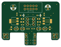
Power breakout
50.8 × 38.7 mm27 parts2LCC-BY-SA-4.023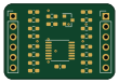
Analog in buffers
27.1 × 18.5 mm23 parts2LCC-BY-SA-4.023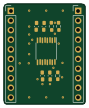
Analog Multiplexer
21.5 × 26.5 mm10 parts2LCC-BY-SA-4.023