
PCIce

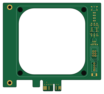
About the PCIce PCB
PCIce is an open source AVR/Arduino PCB design by ZoidTechnology, published on GitHub under the GPL-3.0 license. It is a 2-layer board measuring 110 × 99.6 mm, with 18 components from 11 distinct parts.
Its main chip is the ATTINY13A, from the AVR/Arduino family. Other key parts include the 5V SOT-89 REG. By type, the board carries 5 resistors, 4 diodes, 3 capacitors, 2 ICs, 2 connectors and 1 fuse.
From the project
A PCI Express card with an inbuilt PWM fan controller and mounting points for an 80mm fan.
PCIce is available to buy on Tindie. More information can be found on my website. ## Hardware The hardware is based on an ATtiny13A which outputs a 25kHz PWM signal to the fan. A button is used for speed control, and the current speed is displayed on four multiplexed LEDs. ## Firmware ### Functionality The firmware attempts to load the speed setting from EEPROM on boot. The speed setting is stored twice to guard against corruption. The second copy is inverted to detect a blank EEPROM. The speed will default to maximum if corruption is detected to prevent overheating. The button is debounced…
Main components on the PCIce
PCIce bill of materials (BOM)
18 components, 11 distinct parts.
| Qty | Part | Footprint | Refs |
|---|---|---|---|
| 1 | 5V SOT-89 REG | SOT89-3 | U1 |
| 1 | ATTINY13A | SOIC-8 | U2 |
| 1 | CON 2X3 | GENERIC_IDC_2X3 | J1 |
| 1 | CON 3+1 | 744-81-04TB1B | J2 |
| 1 | 1A | F_1812 | F1 |
| 1 | LPTS | GENERIC_LOW_PROFILE_SWITCH | SW1 |
| 4 | LED | LED_0805 | D1, D2, D3, D4 |
| 2 | 1U | C_0805 | C1, C2 |
| 1 | 100N | C_0805 | C3 |
| 1 | 220 | R_0805 | R1 |
| 4 | 4K7 | R_0805 | R2, R3, R4, R5 |
PCIce design files
The KiCad project lives in the ZoidTechnology/PCIce repository on GitHub; these links point at the commit this page was built from.
- Layouthardware/pcice.kicad_pcb
- Schematichardware/pcice.kicad_sch
PCIce: common questions
What microcontroller does the PCIce use?
The PCIce is built around the ATTINY13A, from the AVR/Arduino family.
How big is the PCIce PCB?
The PCIce measures 110 × 99.6 mm, has 2 copper layers and is 1.6 mm thick.
How many components are on the PCIce?
18 components, from 11 distinct parts. The full bill of materials is listed on this page.
Where can I download the PCIce design files?
From the ZoidTechnology/PCIce repository on GitHub, which has the KiCad layout and the schematic; the links under Design files point to each one.
Can I use the PCIce design in my own project?
Yes, under the terms of its GPL-3.0 license, which ZoidTechnology chose for the repository.
Can I test firmware for the PCIce without the hardware?
Yes. HardLabs builds a simulation of the board from its netlist and BOM, so you can run and debug AVR/Arduino firmware against it before you order a PCB.
Similar boards
 AVR/Arduino
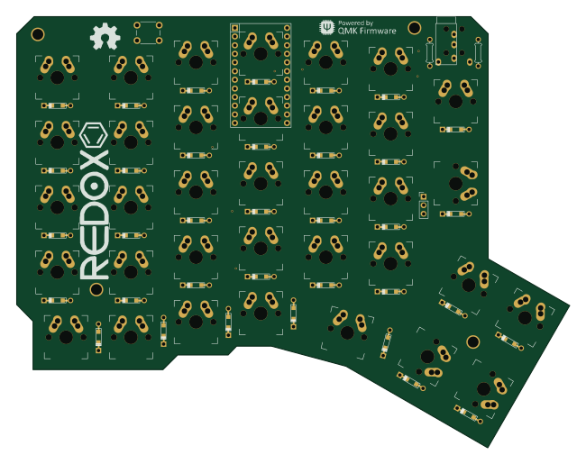
Redox keyboard
mattdibi
162.2 × 126.5 mm77 parts2LMIT2.0k AVR/Arduino
ModuleV450
stuartpittaway
30 × 61.4 mm39 parts2LCC-BY-NC-4.01.1k AVR/Arduino
V4
30 × 50 mm38 parts2LCC-BY-NC-4.01.1k AVR/Arduino
Discipline
coseyfannitutti
304.9 × 122.8 mm170 parts2LCC-BY-NC-4.01.0k AVR/Arduino
Megadesk
gcormier
41.7 × 32.2 mm23 parts2LGPL-3.0818 AVR/Arduino
Easyduino Atmega Nano
Hanqaqa
43.4 × 18 mm30 parts4LCERN-OHL-P-2.0746