
My TechPad

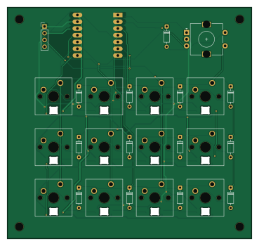
About the My TechPad PCB
My TechPad is an open source PCB design by AB-TheCoder, published on GitHub under the MIT license. It is a 2-layer board measuring 92 × 87 mm, with 40 components from 6 distinct parts.
Other key parts include the MOUDLE-SEEEDUINO-XIAO. By type, the board carries 13 switches, 13 diodes, 12 LEDs, 1 IC and 1 connector.
It belongs with the keyboards and displays & leds designs in this gallery.
From the project
This repo is the main code base for my hackpad project.
- What i plan , is to make a esthetic and slick hackpad which will have a the following features: 1. The hackpad will have rgb lightning and will be connected to a device using wired connection(usb) 2. it will have its own application which will allow to set commands and actions for the button 3. it will be aesthetic black in colour with crazy lighting (customizable through app) 4. i am planning to keep it simple and in devoloper theme. 5. it will be a slick and esthetic desing, with 2 rotatory encoder, a oled screen , 12 keypads 6. i dont plan on using anything extra or of my own . 7. good…
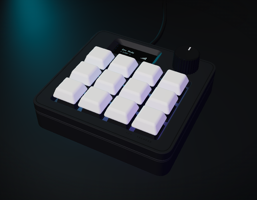
Main components on the My TechPad
My TechPad bill of materials (BOM)
40 components, 6 distinct parts — part numbers from the project's BOM.
| Qty | Part | Footprint | Refs |
|---|---|---|---|
| 1 | MOUDLE-SEEEDUINO-XIAO | XIAO-Generic-Hybrid-14P-2.54-21X17.8MM | U1 |
| 1 | OLED_0.91_SSD1306 | PinHeader_1x04_P2.54mm_Vertical | J1 |
| 12 | SW_Push | SW_Cherry_MX_1.00u_PCB | SW1, SW2, SW3, SW4, SW5, SW6, SW7, SW8 +4 |
| 1 | RotaryEncoder_Switch | RotaryEncoder_Alps_EC11E-Switch_Vertical_H20mm | SW13 |
| 12 | SK6812MINI-E | SK6812MINI-E_fixed | LED1, LED2, LED3, LED4, LED5, LED6, LED7, LED8 +4 |
| 13 | D | D_DO-35_SOD27_P7.62mm_Horizontal | D1, D2, D3, D4, D5, D6, D7, D8 +5 |
My TechPad design files
The KiCad project lives in the AB-TheCoder/My_TechPad repository on GitHub; these links point at the commit this page was built from.
- LayoutPCB/pcb.kicad_pcb
- SchematicPCB/pcb.kicad_sch
- BOMDocumentation/BOM.csv
My TechPad: common questions
How big is the My TechPad PCB?
The My TechPad measures 92 × 87 mm, has 2 copper layers and is 1.6 mm thick.
How many components are on the My TechPad?
40 components, from 6 distinct parts, with part numbers taken from the project's own BOM. The full bill of materials is listed on this page.
Where can I download the My TechPad design files?
From the AB-TheCoder/My_TechPad repository on GitHub, which has the KiCad layout, the schematic and the BOM; the links under Design files point to each one.
Can I use the My TechPad design in my own project?
Yes, under the terms of its MIT license, which AB-TheCoder chose for the repository.
Similar boards
View base
scottbez1
81.2 × 81.2 mm81 parts2LApache-2.022.2k
BM28B0.6-24DSBreakout
15.2 × 35.6 mm3 parts2LApache-2.022.2k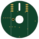
View screen
35 × 35 mm12 parts2LApache-2.022.2k
LevelShifterBreakout
15.2 × 20.3 mm5 parts2LApache-2.022.2k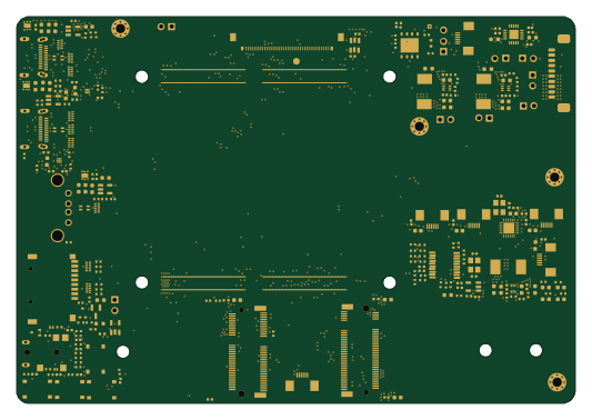
Anyon e motherboard
byrantech
133 × 92 mm258 parts6LMIT4.3k
Switch
18.5 × 11.1 mm5 parts2LMIT4.3k